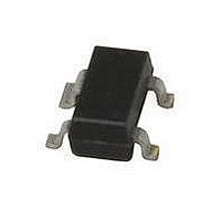
BF1202,215 NXP Semiconductors, BF1202,215 Datasheet

BF1202,215
Specifications of BF1202,215
Related parts for BF1202,215
BF1202,215 Summary of contents
Page 1
DATA SHEET BF1202; BF1202R; BF1202WR N-channel dual-gate PoLo MOS-FETs Product specification Supersedes data of 2000 Mar 29 DISCRETE SEMICONDUCTORS 2010 Sep 16 ...
Page 2
... NXP Semiconductors N-channel dual-gate PoLo MOS-FETs FEATURES Short channel transistor with high forward transfer admittance to input capacitance ratio Low noise gain controlled amplifier Partly internal self-biasing circuit to ensure good cross-modulation performance during AGC and good DC stabilization. APPLICATIONS VHF and UHF applications with ...
Page 3
... NXP Semiconductors N-channel dual-gate PoLo MOS-FETs LIMITING VALUES In accordance with the Absolute Maximum Rating System (IEC 60134). SYMBOL PARAMETER V drain-source voltage DS I drain current D I gate 1 current G1 I gate 2 current G2 P total power dissipation tot BF1202; BF1202R BF1202WR T storage temperature stg ...
Page 4
... NXP Semiconductors N-channel dual-gate PoLo MOS-FETs STATIC CHARACTERISTICS = 25 C unless otherwise specified SYMBOL PARAMETER V drain-source breakdown voltage (BR)DSS V gate 1-source breakdown voltage (BR)G1-SS V gate 2-source breakdown voltage (BR)G2-SS V forward source-gate 1 voltage (F)S-G1 V forward source-gate 2 voltage (F)S-G2 V gate 1-source threshold voltage G1-S(th) ...
Page 5
... NXP Semiconductors N-channel dual-gate PoLo MOS-FETs 20 handbook, halfpage V G2 (mA) 3 0.4 0 Fig.5 Transfer characteristics; typical values. 100 handbook, halfpage V G2 (μ 0 Fig.7 Gate 1 current as a function of gate 1 voltage; typical values. 2010 Sep 16 MCD952 handbook, halfpage 2 1 1.2 1.6 ...
Page 6
... NXP Semiconductors N-channel dual-gate PoLo MOS-FETs 20 handbook, halfpage I D (mA G2 Fig.9 Drain current as a function of gate 1 current; typical values. 20 handbook, halfpage I D (mA G2 connected see Fig.21 Fig.11 Drain current as a function of gate and drain supply voltage; typical values. 2010 Sep 16 ...
Page 7
... NXP Semiconductors N-channel dual-gate PoLo MOS-FETs 40 handbook, halfpage I G1 (μ 120 k (connected see Fig.21 Fig.13 Gate 1 current as a function of gate 2 voltage; typical values. 120 handbook, halfpage V unw (dBμV) 110 100 120 k MHz MHz; T unw amb Fig.15 Unwanted voltage for 1% cross-modulation as a function of gain reduction ...
Page 8
... NXP Semiconductors N-channel dual-gate PoLo MOS-FETs 2 10 handbook, halfpage Y is (mS − mA amb Fig.17 Input admittance as a function of frequency; typical values handbook, halfpage y fs (mS ϕ mA amb Fig.19 Forward transfer admittance and phase as a function of frequency; typical values. 2010 Sep 16 MCD964 ...
Page 9
... NXP Semiconductors N-channel dual-gate PoLo MOS-FETs handbook, full pagewidth R GEN 50 Ω Table 1 Scattering parameters MAGNITUDE ANGLE (MHz) (ratio) (deg) 3.26 50 0.988 6.52 100 0.988 12.99 200 0.984 19.39 300 0.977 25.65 400 0.965 31.76 500 0.951 37.68 600 0.936 43.42 700 0.919 ...
Page 10
... NXP Semiconductors N-channel dual-gate PoLo MOS-FETs PACKAGE OUTLINES Plastic surface-mounted package; 4 leads DIMENSIONS (mm are the original dimensions UNIT max 1.1 0.48 0.88 0.1 mm 0.9 0.38 0.78 OUTLINE VERSION IEC SOT143B 2010 Sep scale 0.15 3.0 1.4 1.9 1.7 0.09 2.8 1.2 ...
Page 11
... NXP Semiconductors N-channel dual-gate PoLo MOS-FETs Plastic surface-mounted package; reverse pinning; 4 leads DIMENSIONS (mm are the original dimensions UNIT max 1.1 0.48 0.88 0.1 mm 0.9 0.38 0.78 OUTLINE VERSION IEC SOT143R 2010 Sep scale 0.15 3.0 1.4 1.9 1.7 0.09 2.8 1.2 ...
Page 12
... NXP Semiconductors N-channel dual-gate PoLo MOS-FETs Plastic surface-mounted package; reverse pinning; 4 leads DIMENSIONS (mm are the original dimensions UNIT max 0.4 1.1 0.7 mm 0.1 0.3 0.5 0.8 OUTLINE VERSION IEC SOT343R 2010 Sep scale 0.25 2.2 1.35 1.3 1.15 0.10 1.8 1.15 ...
Page 13
... In no event shall NXP Semiconductors be liable for any indirect, incidental, punitive, special or consequential damages (including - without limitation - lost profits, lost savings, business interruption, costs related to the ...
Page 14
... NXP Semiconductors’ specifications such use shall be solely at customer’s own risk, and (c) customer fully indemnifies NXP Semiconductors for any liability, damages or failed product claims resulting from customer design and use of the product for automotive applications beyond NXP Semiconductors’ ...
Page 15
... Interface, Security and Digital Processing expertise Customer notification This data sheet was changed to reflect the new company name NXP Semiconductors, including new legal definitions and disclaimers. No changes were made to the technical content, except for the marking codes and the package outline drawings which were updated to the latest version. ...


