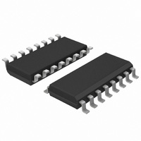
UJA1023T/2R04,512 NXP Semiconductors, UJA1023T/2R04,512 Datasheet - Page 5

UJA1023T/2R04,512
Manufacturer Part Number
UJA1023T/2R04,512
Description
IC CAN/LIN I/O SLAVE 32HTSSOP
Manufacturer
NXP Semiconductors
Datasheet
1.UJA1023T2R04C51.pdf
(49 pages)
Specifications of UJA1023T/2R04,512
Applications
LIN Controller
Interface
LIN (Local Interconnect Network)
Voltage - Supply
6.5 V ~ 27 V
Package / Case
16-SOIC (3.9mm Width)
Mounting Type
Surface Mount
Lead Free Status / RoHS Status
Lead free / RoHS Compliant
Other names
935281302512
UJA1023T/2R04
UJA1023T/2R04
UJA1023T/2R04
UJA1023T/2R04
NXP Semiconductors
7. Functional description
UJA1023
Product data sheet
7.1.1 LIN controller
7.1.2 LIN transceiver (including termination)
7.1.3 Automatic bit rate detection
7.1.4 Oscillator
7.1.5 I/O block
7.1.6 ADC
7.1.7 PWM
7.1 Short description of the UJA1023
The UJA1023 combines all blocks necessary to work as a stand-alone LIN slave. Various
I/O functions typically used in a car are supported. For a more detailed description refer to
Section 7.2
The LIN 2.0 controller monitors and evaluates the LIN messages in order to process the
LIN commands. It supervises and executes the NAD assignment, ID assignment and
I/O-configuration and controls the operating modes of the UJA1023.
The NAD configuration is done by a combination of a LIN master request frame and a
setting done by either a daisy chain or plug ID code.
The LIN transceiver, which is LIN 2.0 / SAE J2602 compliant, is the interface between the
internal LIN controller and the physical LIN bus. The transmit data stream of the LIN
controller is converted into a bus signal with an optimized wave shape to minimize
electromagnetic emission. The required LIN slave termination of 30 kΩ is already
integrated. In case of LIN bus faults the UJA1023 switches to the low-power Limp home
mode.
The automatic bit rate detection adapts to the LIN master’s bit rate. Any bit rate between
1 kbit/s and 20 kbit/s can be handled. This block checks whether the synchronization
break and synchronization field are valid. If not, the message will be rejected.
The on-chip oscillator provides the internal clock signal for some digital functions and is
the time reference for the automatic bit rate detection.
The I/O block controls the configuration of the I/O pins. The LIN master configures the I/O
pin functionality by means of a master request frame and an optional slave response
frame.
Besides the standard level input and output behavior the following functions are also
handled by the UJA1023: local wake-up, cyclic input, edge capture, PWM output, switch
matrix I/O and AD conversion.
With three external components an 8-bit ADC function can be implemented. Each of the
eight bidirectional I/O pins can be used as input for the ADC, one at a time.
Each pin can be configured with a Pulse Width Modulation (PWM) function. The resolution
is 8-bit and the base frequency is approximately 2.7 kHz.
to
Section
All information provided in this document is subject to legal disclaimers.
7.6. The block diagram is shown in
Rev. 5 — 17 August 2010
Figure
1.
UJA1023
© NXP B.V. 2010. All rights reserved.
LIN-I/O slave
5 of 49


