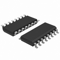
UJA1023T/2R04,512 NXP Semiconductors, UJA1023T/2R04,512 Datasheet - Page 21

UJA1023T/2R04,512
Manufacturer Part Number
UJA1023T/2R04,512
Description
IC CAN/LIN I/O SLAVE 32HTSSOP
Manufacturer
NXP Semiconductors
Datasheet
1.UJA1023T2R04C51.pdf
(49 pages)
Specifications of UJA1023T/2R04,512
Applications
LIN Controller
Interface
LIN (Local Interconnect Network)
Voltage - Supply
6.5 V ~ 27 V
Package / Case
16-SOIC (3.9mm Width)
Mounting Type
Surface Mount
Lead Free Status / RoHS Status
Lead free / RoHS Compliant
Other names
935281302512
UJA1023T/2R04
UJA1023T/2R04
UJA1023T/2R04
UJA1023T/2R04
NXP Semiconductors
UJA1023
Product data sheet
Table 23.
[1]
Table 24.
[1]
Data
byte
D0
D1
D2
D3
D4
D5
D6
D7
Byte
D0
D1
D2
D3
D4
D5
D6 and D7 7 to 0
[1]
Undefined.
All diagnosis flags in byte D4 are reset after data access from master.
7
NAD7
0
1
1
P
PL7
1
1
Fourth I/O diagnostic data block response frame bit allocation
Fourth I/O diagnostic data block response frame bit description
Bit
7 to 0
7 to 0
7 to 0
7 and 6
5 to 0
7
6
5
4
3
2
1
0
7 to 0
All information provided in this document is subject to legal disclaimers.
6
NAD6
0
1
1
RxB
PL6
1
1
Rev. 5 — 17 August 2010
Symbol
NAD[7:0]
PCI[7:0]
RSID[7:0]
-
-
P
RxB
CS
TxB
undefined
NVM
LHE
ERR
PL[7:0]
-
5
NAD5
0
1
0
CS
PL5
1
1
Slave node address (NAD). NAD values are in the range
Protocol control information.
Receive error. Set if start or stop bits are erroneous during
Transmit error. Set if start, data or stop bits are erroneous
-
No valid message. Set if there is bus activity, but no valid
PxOut latch value.
Description
from 1 to 127, while 0 and 128 to 255 are reserved for other
purposes. The slave node address is assigned with the
assign NAD command (see
Response service identifier.
11 for the fourth configuration data block.
Not used.
Parity error. Set if identifier parity bits are erroneous.
reception.
Checksum error. Set if checksum is erroneous.
during transmission.
message frame for longer than t
Set if Limp home mode is entered.
Response error. Sets internal signal Response_Error if there
is an RxB, CS or TxB during a response frame.
Not used.
4
NAD4
0
1
0
TxB
PL4
1
1
3
NAD3
0
0
0
u
PL3
1
1
[1]
2
NAD2
1
1
0
NVM
PL2
1
1
Table
1
NAD1
0
0
0
LHE
PL1
1
1
to(idle)
5).
.
UJA1023
© NXP B.V. 2010. All rights reserved.
0
NAD0
0
0
0
ERR
PL0
1
1
LIN-I/O slave
Default
value
(hex)
NAD
04
F4
C0
00
00
FF
FF
21 of 49


