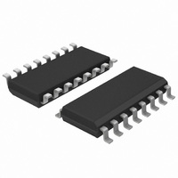
UJA1023T/2R04,512 NXP Semiconductors, UJA1023T/2R04,512 Datasheet - Page 16

UJA1023T/2R04,512
Manufacturer Part Number
UJA1023T/2R04,512
Description
IC CAN/LIN I/O SLAVE 32HTSSOP
Manufacturer
NXP Semiconductors
Datasheet
1.UJA1023T2R04C51.pdf
(49 pages)
Specifications of UJA1023T/2R04,512
Applications
LIN Controller
Interface
LIN (Local Interconnect Network)
Voltage - Supply
6.5 V ~ 27 V
Package / Case
16-SOIC (3.9mm Width)
Mounting Type
Surface Mount
Lead Free Status / RoHS Status
Lead free / RoHS Compliant
Other names
935281302512
UJA1023T/2R04
UJA1023T/2R04
UJA1023T/2R04
UJA1023T/2R04
NXP Semiconductors
UJA1023
Product data sheet
7.2.1.5 I/O configuration
Table 14.
The I/O configuration is done via the LIN configuration request ‘Data Dump’, where the
first data byte of the MasterReq contains the slave node address NAD. The I/O-pin
configuration process starts only, if the received slave node address matches the own
UJA1023 node address and if data byte D2 (SID) is 0xB4.
As with the other configuration commands, the master transmits the I/O-pin configuration
data via the MasterReq message. Due to the limited amount of data bytes within the LIN
configuration command ‘Data Dump’, the configuration and diagnosis is split-up into four
blocks. The configuration and diagnosis blocks are distinguished on bits 6 and 7 of data
byte D3. The master can review the new configuration data via the SlaveResp message.
Finally if the master considers the received configuration data of the LIN-I/O to be correct,
it can enable the slave I/O-configuration by using the UJA1023 message frames (see
Section
It should be noted that for correct I/O configuration, the configuration requests must be
sent in sequential order of: first, second and third configuration data block.
Table 15.
Data
byte
D0
D1
D2
D3
D4
D5
D6
D7
Data
byte
D0
D1
D2
D3
D4
D5
D6
D7
7.2.5) PxResp or PxReq.
OM0_7
OM1_7
7
NAD7
0
0
1
0
1
1
1
7
NAD7
0
1
0
HSE7
LSE7
Read by identifier negative response
First I/O configuration data block bit allocation
All information provided in this document is subject to legal disclaimers.
6
NAD6
0
1
0
0
1
1
1
6
NAD6
0
0
0
HSE6
LSE6
OM0_6
OM1_6
Rev. 5 — 17 August 2010
5
NAD5
0
1
1
0
1
1
1
5
NAD5
0
1
IM1
HSE5
LSE5
OM0_5
OM1_5
4
NAD4
0
1
1
1
1
1
1
4
NAD4
0
1
IM0
HSE4
LSE4
OM0_4
OM1_4
3
NAD3
0
1
0
0
1
1
1
3
NAD3
0
0
RxDL
HSE3
LSE3
OM0_3
OM1_3
2
NAD2
0
1
0
0
1
1
1
2
NAD2
1
1
ADCIN2 ADCIN1 ADCIN0 00
HSE2
LSE2
OM0_2
OM1_2
1
NAD1
1
1
1
1
1
1
1
1
NAD1
1
0
HSE1
LSE1
OM0_1
OM1_1
UJA1023
© NXP B.V. 2010. All rights reserved.
0
NAD0
1
1
0
0
1
1
1
0
NAD0
0
0
HSE0
LSE0
OM0_0
OM1_0
LIN-I/O slave
Default
value
(hex)
NAD
03
7F
B2
12
FF
FF
FF
Default
value
(hex)
NAD
06
B4
00
00
00
00
16 of 49


