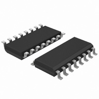
UJA1023T/2R04,512 NXP Semiconductors, UJA1023T/2R04,512 Datasheet - Page 30

UJA1023T/2R04,512
Manufacturer Part Number
UJA1023T/2R04,512
Description
IC CAN/LIN I/O SLAVE 32HTSSOP
Manufacturer
NXP Semiconductors
Datasheet
1.UJA1023T2R04C51.pdf
(49 pages)
Specifications of UJA1023T/2R04,512
Applications
LIN Controller
Interface
LIN (Local Interconnect Network)
Voltage - Supply
6.5 V ~ 27 V
Package / Case
16-SOIC (3.9mm Width)
Mounting Type
Surface Mount
Lead Free Status / RoHS Status
Lead free / RoHS Compliant
Other names
935281302512
UJA1023T/2R04
UJA1023T/2R04
UJA1023T/2R04
UJA1023T/2R04
NXP Semiconductors
UJA1023
Product data sheet
Table 25.
[1]
Table 26.
[1]
Data
byte
D0
D1
D2
Byte
D0
D1
D2
Fig 9.
[1]
[1]
The UJA1023 expects to receive data byte D2 only if bit RxDL = 1 (bit 3 of byte D3 in the first I/O
configuration data block, see
The UJA1023 expects to receive data byte D2 only if bit RxDL = 1 (bit 3 of byte D3 in the first I/O
configuration data block, see
up/down
oscillator
7
P7
PWM7
-
Analog-to-digital converter
Bit
7 to 0
7 to 0
7 to 3
2 to 0
PxReq frame bit allocation
PxReq frame bit description
All information provided in this document is subject to legal disclaimers.
REGISTER/COUNTER
FF
6
P6
PWM6
-
Symbol
P[7:0]
PWM[7:0]
-
ADCIN[2:0]
COUNTER
Rev. 5 — 17 August 2010
oscillator
5
P5
PWM5
-
Table 15
Table 15
T
FILTER
Description
Px output value. The Px output value is ignored if Px is
configured in cyclic sense or PWM mode.
PWM value.
Not used.
ADC analog source channel selection. For example, 000
selects input 0, 001 selects input 1 and 111 selects input 7. The
ADC input source is observed only if the INH output is in ADC
mode.
and
and
4
P4
PWM4
-
ADC
period
Table
Table
0.5V VIO
16).
16).
3
P3
PWM3
-
mode
ADC
MUX
2
P2
PWM2
ADCIN2 ADCIN1 ADCIN0 00
V
VIO
1
P1
PWM1
INH
Px
UJA1023
© NXP B.V. 2010. All rights reserved.
0
P0
PWM0
R i
100 kΩ
C1
10 nF
LIN-I/O slave
100 kΩ
R1
mdb497
Default
value
(hex)
00
00
30 of 49
V
A


