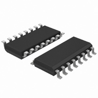
UJA1023T/2R04,512 NXP Semiconductors, UJA1023T/2R04,512 Datasheet - Page 40

UJA1023T/2R04,512
Manufacturer Part Number
UJA1023T/2R04,512
Description
IC CAN/LIN I/O SLAVE 32HTSSOP
Manufacturer
NXP Semiconductors
Datasheet
1.UJA1023T2R04C51.pdf
(49 pages)
Specifications of UJA1023T/2R04,512
Applications
LIN Controller
Interface
LIN (Local Interconnect Network)
Voltage - Supply
6.5 V ~ 27 V
Package / Case
16-SOIC (3.9mm Width)
Mounting Type
Surface Mount
Lead Free Status / RoHS Status
Lead free / RoHS Compliant
Other names
935281302512
UJA1023T/2R04
UJA1023T/2R04
UJA1023T/2R04
UJA1023T/2R04
NXP Semiconductors
Table 33.
V
unless otherwise specified.
[1]
[2]
[3]
[4]
[5]
[6]
[7]
[8]
UJA1023
Product data sheet
Symbol
t
LIN protocol controller
t
t
t
t
t
Automatic bit rate detection
t
f
Cyclic function; see
T
t
t
ADC function
E
P(RX)(sym)
to(idle)
to(dom)
to(rec)
wake(bus)
wake(local)
det(syncbrk)
tol(sync)
on(PxOut)
sample(PxIn)
BAT
cy
ADC
All parameters are guaranteed over the virtual junction temperature range by design. Products are 100 % tested at 125 °C ambient
temperature on wafer level (pre-testing). Cased products are 100 % tested at 25 °C ambient temperature (final testing). Both pre-testing
and final testing use correlated test conditions to cover the specified temperature and power supply voltage ranges.
Guaranteed by design.
Analog-to-digital conversion starts when valid sync break and sync field is received.
t
and R
RXD is an internal signal.
Not tested.
δ
δ
bit
= 5.5 V to 27 V; V
1
2
,
,
= selected bit time 50 μs or 96 μs (20 kbit/s or 10.4 kbit/s), depends on LSC bit; bus load conditions are (C parallel to R): C
δ
δ
3
4
bus
=
=
Dynamic characteristics
= 1 kΩ, C
t
------------------------------ -
t
------------------------------- -
Parameter
symmetry of receiver
propagation delay rising
edge with respect to falling
edge
bus idle time-out
bus dominant time-out
bus recessive time-out
network wake-up signal
time
bus wake-up dominant
time
sync break detection
threshold
total tolerance slave
synchronized
cycle period
PxOut pin turned on
PxIn sample time
total ADC error
bus rec
bus rec
2 t
2 t
(
(
×
×
) min
) max
bit
bit
(
(
bus
Figure 7
VIO
= 6.8 nF and R
)
)
= 3 V to 27 V; T
[1]
bus
…continued
= 660 Ω or C
vj
All information provided in this document is subject to legal disclaimers.
R = 100 kΩ; C = 10 nF
Conditions
after local wake-up, sent by slave
Sleep mode, sent by master
complete message
=
V
V
V
V
−
VIO
BAT
VIO
BAT
40
°
Rev. 5 — 17 August 2010
= 6.5 V to 12 V;
= 3 V to 27 V;
= 6.5 V to 12 V
= 6.5 V to 27 V
C to +150
bus
= 10 nF and R
°
C; R
L(LIN-BAT)
bus
= 500 Ω.
= 500
[7]
[2]
[2]
[2]
[2]
[2]
[4]
[2]
[2]
[2]
[8]
[8]
Ω
; all voltages are referenced to GND;
-
Min
−2
4.1
32
15
0.25
30
-
-
-
-
-
-
Typ
-
-
-
-
-
100
10 × t
-
16
350
262
-
-
bit
UJA1023
© NXP B.V. 2010. All rights reserved.
Max
+2
18.0
270
65
5
150
-
2
-
-
-
4
6
LIN-I/O slave
bus
ms
Unit
μs
s
ms
μs
μs
μs
%
ms
μs
μs
LSB
LSB
40 of 49
= 1 nF


