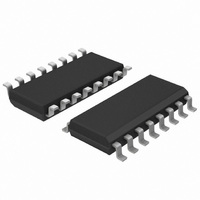
UJA1023T/2R04,512 NXP Semiconductors, UJA1023T/2R04,512 Datasheet - Page 29

UJA1023T/2R04,512
Manufacturer Part Number
UJA1023T/2R04,512
Description
IC CAN/LIN I/O SLAVE 32HTSSOP
Manufacturer
NXP Semiconductors
Datasheet
1.UJA1023T2R04C51.pdf
(49 pages)
Specifications of UJA1023T/2R04,512
Applications
LIN Controller
Interface
LIN (Local Interconnect Network)
Voltage - Supply
6.5 V ~ 27 V
Package / Case
16-SOIC (3.9mm Width)
Mounting Type
Surface Mount
Lead Free Status / RoHS Status
Lead free / RoHS Compliant
Other names
935281302512
UJA1023T/2R04
UJA1023T/2R04
UJA1023T/2R04
UJA1023T/2R04
NXP Semiconductors
UJA1023
Product data sheet
7.2.4 INH pin mode
7.2.5 LIN-I/O message frames
The inverted bit stream of the ADC comparator generates the quasi-analog output voltage
on pin INH, which can be used to control the analog voltage V
An analog-to-digital conversion will have following steps:
To reduce current consumption, the 0.5V
low-power modes.
The External regulator mode, IM0 = IM1 = 0 (see
external voltage regulator. In Configuration mode, Normal mode and Standby mode the
INH outputs a HIGH level, and in the low-power modes (Sleep, LH sleep and Limp home)
the INH pin becomes high-impedance.
Switching between the INH modes ‘external regulator’ and ‘switch open’ the INH pin can
be used as high-side switch.
In ADC mode the INH pin is configured internally as follows: the high-side switch is put in
high-impedance state and a special symmetrical push-pull output is activated. Next, the
ADC mode enables an ADC control loop. The output level of the push-pull stage is
defined via the V
The UJA1023 uses one LIN command to receive data PxReq and one to transmit data
PxResp respectively. The IDs for PxReq and PxResp are configured by means of the
‘assign frame ID’ command as described in
Please note that the I/O configuration will be enabled during the first usage of the PxResp
or PxReq.
The PxReq and PxResp data bytes are described in
1. Select an input channel via PxReq, see
2. The internal multiplexer switches over to the selected input; note that some time is
3. In case a valid sync break and sync field is received, an analog-to-digital conversion
ADC-input is selected (see
needed to stabilize the loop, due to the RC network time constant.
starts. The data is available in the next LIN message, implying the ADC value is
sampled during the previous LIN message.
All information provided in this document is subject to legal disclaimers.
VIO
voltage.
Rev. 5 — 17 August 2010
Table 16
for RxDL = 0 and ADCIN[2:0]).
VIO
Section
Section
reference voltage is turned off in the
Table
7.2.1.3.
7.2.5. Not needed in case a fixed
Table 25
16), can be used to control an
A
to
via a low-pass filter.
Table
UJA1023
28.
© NXP B.V. 2010. All rights reserved.
LIN-I/O slave
29 of 49


