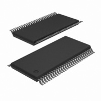
PCA9698DGG/S911,51 NXP Semiconductors, PCA9698DGG/S911,51 Datasheet - Page 9

PCA9698DGG/S911,51
Manufacturer Part Number
PCA9698DGG/S911,51
Description
IC I/O EXPANDER I2C 40B 56TSSOP
Manufacturer
NXP Semiconductors
Datasheet
1.PCA9698BS118.pdf
(48 pages)
Specifications of PCA9698DGG/S911,51
Interface
I²C
Number Of I /o
40
Interrupt Output
Yes
Frequency - Clock
1MHz
Voltage - Supply
2.3 V ~ 5.5 V
Operating Temperature
-40°C ~ 85°C
Mounting Type
Surface Mount
Package / Case
56-TSSOP
Includes
POR
For Use With
OM6281 - DAUGHTER CARD PCA9698 FOR OM6275
Lead Free Status / RoHS Status
Lead free / RoHS Compliant
Other names
935285491518
PCA9698DGG/S911-T
PCA9698DGG/S911-T
PCA9698DGG/S911-T
PCA9698DGG/S911-T
NXP Semiconductors
Table 3.
PCA9698
Product data sheet
Reg #
Input Port registers
00h
01h
02h
03h
04h
05h
06h
07h
D5
0
0
0
0
0
0
0
0
Register summary
7.3.1 5-bank register category
7.3.2 1-bank register category
D4
0
0
0
0
0
0
0
0
7.4 Register definitions
If the Auto-Increment flag is set (AI = 1), the 3 least significant bits are automatically
incremented after a read or write. This allows the user to program and/or read the
5 register banks sequentially.
If more than 5 bytes of data are written and AI = 1, previous data in the selected registers
will be overwritten or reread. Reserved registers are skipped and not accessed (refer to
Table
If the Auto-Increment flag is cleared (AI = 0), the 3 least significant bits are not
incremented after data is read or written, only one register will be repeatedly read or
written.
If more than 1 byte of data is written or read, previous data in the same register is
overwritten independently of the value of AI.
D3
0
0
0
0
0
0
0
0
•
•
•
•
•
•
•
•
IP – Input registers
OP – Output registers
PI – Polarity Inversion registers
IOC – I/O Configuration registers
MSK – Mask interrupt registers
OUTCONF – Output Structure Configuration register
ALLBNK – All Bank Control register
MODE – Mode Selection register
3).
D2
0
0
0
0
1
1
1
1
D1
0
0
1
1
0
0
1
1
All information provided in this document is subject to legal disclaimers.
D0
0
1
0
1
0
1
0
1
40-bit Fm+ I
Rev. 3 — 3 August 2010
Name
IP0
IP1
IP2
IP3
IP4
-
-
-
2
C-bus advanced I/O port with RESET, OE and INT
Type
read only
read only
read only
read only
read only
-
-
-
Function
Input Port register bank 0
Input Port register bank 1
Input Port register bank 2
Input Port register bank 3
Input Port register bank 4
reserved for future use
reserved for future use
reserved for future use
PCA9698
© NXP B.V. 2010. All rights reserved.
9 of 48


