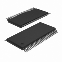
PCA9698DGG/S911,51 NXP Semiconductors, PCA9698DGG/S911,51 Datasheet - Page 18

PCA9698DGG/S911,51
Manufacturer Part Number
PCA9698DGG/S911,51
Description
IC I/O EXPANDER I2C 40B 56TSSOP
Manufacturer
NXP Semiconductors
Datasheet
1.PCA9698BS118.pdf
(48 pages)
Specifications of PCA9698DGG/S911,51
Interface
I²C
Number Of I /o
40
Interrupt Output
Yes
Frequency - Clock
1MHz
Voltage - Supply
2.3 V ~ 5.5 V
Operating Temperature
-40°C ~ 85°C
Mounting Type
Surface Mount
Package / Case
56-TSSOP
Includes
POR
For Use With
OM6281 - DAUGHTER CARD PCA9698 FOR OM6275
Lead Free Status / RoHS Status
Lead free / RoHS Compliant
Other names
935285491518
PCA9698DGG/S911-T
PCA9698DGG/S911-T
PCA9698DGG/S911-T
PCA9698DGG/S911-T
NXP Semiconductors
PCA9698
Product data sheet
7.10 Interrupt output (INT)
7.8 Power-on reset
7.9 RESET input
Remark: After programming a PCA9698, its state machine will be in a
‘wait-for-STOP-condition’ until a STOP condition is received to update the Output Port
registers. Since this state machine will be in a ‘wait-state’, the part will not respond to its
own address until this state machine gets out to the idle condition, which means that the
device can be programmed only once and is not addressable again until a STOP
condition has been received.
Remark: The PCA9698 has one level of buffers to store 5 bytes of data, and the actual
Output Port registers will get updated on the STOP condition. If the master sends more
than 5 bytes of data (with AI = 1), the data in the buffer will get overwritten.
When power is applied to V
a reset condition until V
and the PCA9698 registers and I
states. Thereafter, V
A reset can be accomplished by holding the RESET pin LOW for a minimum of t
PCA9698 registers and I
RESET input is once again HIGH.
The open-drain active LOW interrupt is activated when one of the port pins changes state
and the port pin is configured as an input and the interrupt on it is not masked. The
interrupt is deactivated when the port pin input returns to its previous state or the Input
Port register is read.
It is highly recommended to program the MSK register, and the IOC registers during the
initialization sequence after power-up, since any change to them during Normal mode
operation may cause undesirable interrupt events to happen.
Remark: Changing an I/O from an output to an input may cause a false interrupt to occur
if the state of the pin does not match the contents of the Input Port register.
Only a Read of the Input Port register that contains the bit(s) image of the input(s) that
generated the interrupt clears the interrupt condition.
If more than one input register changed state before a read of the Input Port register is
initiated, the interrupt is cleared when all the input registers containing all the inputs that
changed are read.
Example: If IO0_5, IO2_3, and IO3_7 change state at the same time, the interrupt is
cleared only when INREG0, INREG2, and INREG3 are read.
•
•
When all the devices have been accessed, the master must generate a STOP
command.
At the STOP command, all the PCA9698s that have been accessed will update their
Output Port registers that have been programmed and change the output states all at
the same time.
All information provided in this document is subject to legal disclaimers.
DD
40-bit Fm+ I
Rev. 3 — 3 August 2010
DD
must be lowered below 0.2 V to reset the device.
2
C-bus state machine will be held in their default state until the
has reached V
DD
, an internal Power-On Reset (POR) holds the PCA9698 in
2
C-bus/SMBus state machine will initialize to their default
2
C-bus advanced I/O port with RESET, OE and INT
POR
. At that point, the reset condition is released
PCA9698
© NXP B.V. 2010. All rights reserved.
w(rst)
18 of 48
. The


