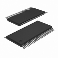
PCA9698DGG/S911,51 NXP Semiconductors, PCA9698DGG/S911,51 Datasheet - Page 38

PCA9698DGG/S911,51
Manufacturer Part Number
PCA9698DGG/S911,51
Description
IC I/O EXPANDER I2C 40B 56TSSOP
Manufacturer
NXP Semiconductors
Datasheet
1.PCA9698BS118.pdf
(48 pages)
Specifications of PCA9698DGG/S911,51
Interface
I²C
Number Of I /o
40
Interrupt Output
Yes
Frequency - Clock
1MHz
Voltage - Supply
2.3 V ~ 5.5 V
Operating Temperature
-40°C ~ 85°C
Mounting Type
Surface Mount
Package / Case
56-TSSOP
Includes
POR
For Use With
OM6281 - DAUGHTER CARD PCA9698 FOR OM6275
Lead Free Status / RoHS Status
Lead free / RoHS Compliant
Other names
935285491518
PCA9698DGG/S911-T
PCA9698DGG/S911-T
PCA9698DGG/S911-T
PCA9698DGG/S911-T
NXP Semiconductors
[2]
[3]
[4]
[5]
[6]
[7]
PCA9698
Product data sheet
Fig 37. Definition of timing on the I
Fig 38. I
t
Minimum SCL clock frequency is limited by the bus time-out feature, which resets the serial bus interface if either SDA or SCL is held
LOW for a minimum of 25 ms. Disable bus time-out feature for DC operation.
A master device must internally provide a hold time of at least 300 ns for the SDA signal (refer to the V
bridge the undefined region of SCL’s falling edge.
C
The maximum t
250 ns. This allows series protection resistors to be connected between the SDA and the SCL pins and the SDA/SCL bus lines without
exceeding the maximum specified t
Input filters on the SDA and SCL inputs suppress noise spikes less than 50 ns.
VD;DAT
b
SDA
SCL
= total capacitance of one bus line in pF.
Rise and fall times refer to V
= minimum time for SDA data out to be valid following SCL LOW.
2
C-bus timing diagram
P
t
BUF
protocol
f
SDA
SCL
for the SDA and SCL bus lines is specified at 300 ns. The maximum fall time for the SDA output stage t
S
t
SU;STA
t
t
HD;STA
BUF
condition
t
LOW
START
(S)
t
HD;STA
IL
f
.
and V
2
t
t
t
LOW
r
HD;DAT
C-bus
t
r
All information provided in this document is subject to legal disclaimers.
IH
MSB
bit 7
(A7)
.
t
HIGH
40-bit Fm+ I
Rev. 3 — 3 August 2010
t
t
HIGH
SU;DAT
t
f
1
/f
bit 6
(A6)
SCL
t
f
t
HD;DAT
t
SU;DAT
2
C-bus advanced I/O port with RESET, OE and INT
(R/W)
bit 0
t
VD;DAT
acknowledge
Sr
(A)
t
SU;STA
t
HD;STA
t
VD;ACK
condition
STOP
(P)
IL
t
SU;STO
of the SCL signal) in order to
002aab175
t
SP
t
SU;STO
PCA9698
© NXP B.V. 2010. All rights reserved.
002aaa986
f
is specified at
P
38 of 48


