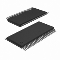
PCA9698DGG/S911,51 NXP Semiconductors, PCA9698DGG/S911,51 Datasheet - Page 2

PCA9698DGG/S911,51
Manufacturer Part Number
PCA9698DGG/S911,51
Description
IC I/O EXPANDER I2C 40B 56TSSOP
Manufacturer
NXP Semiconductors
Datasheet
1.PCA9698BS118.pdf
(48 pages)
Specifications of PCA9698DGG/S911,51
Interface
I²C
Number Of I /o
40
Interrupt Output
Yes
Frequency - Clock
1MHz
Voltage - Supply
2.3 V ~ 5.5 V
Operating Temperature
-40°C ~ 85°C
Mounting Type
Surface Mount
Package / Case
56-TSSOP
Includes
POR
For Use With
OM6281 - DAUGHTER CARD PCA9698 FOR OM6275
Lead Free Status / RoHS Status
Lead free / RoHS Compliant
Other names
935285491518
PCA9698DGG/S911-T
PCA9698DGG/S911-T
PCA9698DGG/S911-T
PCA9698DGG/S911-T
NXP Semiconductors
3. Applications
PCA9698
Product data sheet
2.3 V to 5.5 V operation with 5.5 V tolerant I/Os
40 configurable I/O pins that default to inputs at power-up
Outputs:
Inputs:
Active LOW SMBus Alert (SMBALERT) output pin allows to initiate SMBus ‘Alert
Response Address’ sequence. Own slave address sent when sequence initiated.
Active LOW Reset (RESET) input pin resets device to power-up default state
GPIO All Call address allows programming of more than one device at the same time
with the same parameters
64 programmable slave addresses using 3 address pins
Readable Device ID (manufacturer, device type and revision)
Designed for live insertion in PICMG applications
Low standby current
−40 °C to +85 °C operation
ESD protection exceeds 2000 V HBM per JESD22-A114, 200 V MM per
JESD22-A115, and 1000 V CDM per JESD22-C101
Latch-up testing is done to JEDEC Standard JESD78 which exceeds 100 mA
Packages offered: TSSOP56, and HVQFN56
Servers
RAID systems
Industrial control
Medical equipment
PLCs
Cell phones
Gaming machines
Instrumentation and test measurement
Programmable totem-pole (10 mA source, 25 mA sink) or open-drain (25 mA sink)
with controlled edge rate output structure. Default to totem-pole on power-up.
Active LOW Output Enable (OE) input pin 3-states all outputs. Polarity can be
programmed to active HIGH through the I
Output state change programmable on the Acknowledge or the STOP Command to
update outputs byte-by-byte or all at the same time respectively. Defaults to
Acknowledge on power-up.
Open-drain active LOW Interrupt (INT) output pin allows monitoring of logic level
change of pins programmed as inputs
Programmable Interrupt Mask Control for input pins that do not require an interrupt
when their states change
Polarity Inverter register allows inversion of the polarity of the I/O pins when read
Minimize line disturbance (I
Signal transient rejection (50 ns noise filter and robust I
All information provided in this document is subject to legal disclaimers.
40-bit Fm+ I
Rev. 3 — 3 August 2010
OFF
2
C-bus advanced I/O port with RESET, OE and INT
and power-up 3-state)
2
C-bus. Defaults to OE on power-up.
2
C-bus state machine)
PCA9698
© NXP B.V. 2010. All rights reserved.
2 of 48


