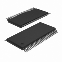
PCA9698DGG/S911,51 NXP Semiconductors, PCA9698DGG/S911,51 Datasheet - Page 8

PCA9698DGG/S911,51
Manufacturer Part Number
PCA9698DGG/S911,51
Description
IC I/O EXPANDER I2C 40B 56TSSOP
Manufacturer
NXP Semiconductors
Datasheet
1.PCA9698BS118.pdf
(48 pages)
Specifications of PCA9698DGG/S911,51
Interface
I²C
Number Of I /o
40
Interrupt Output
Yes
Frequency - Clock
1MHz
Voltage - Supply
2.3 V ~ 5.5 V
Operating Temperature
-40°C ~ 85°C
Mounting Type
Surface Mount
Package / Case
56-TSSOP
Includes
POR
For Use With
OM6281 - DAUGHTER CARD PCA9698 FOR OM6275
Lead Free Status / RoHS Status
Lead free / RoHS Compliant
Other names
935285491518
PCA9698DGG/S911-T
PCA9698DGG/S911-T
PCA9698DGG/S911-T
PCA9698DGG/S911-T
NXP Semiconductors
PCA9698
Product data sheet
Fig 6.
0
0
Alert Response address
0
1
7.2 Alert response, GPIO All Call and Device ID addresses
7.3 Command register
1
Three other different addresses can be sent to the PCA9698.
Following the successful acknowledgement of the slave address + R/W bit, the bus
master will send a byte to the PCA9698, which will be stored in the Command register.
The lowest 6 bits are used as a pointer to determine which register will be accessed.
Registers are divided into 2 categories: 5-bank register category, and 1-bank register
category.
Only a command register code with the 7 least significant bits equal to the 28 allowable
values as defined in
undefined command codes will not be acknowledged. At power-up, this register defaults
to 80h, with the AI bit set to ‘1’, and the lowest 7 bits set to ‘0'.
During a write operation, the PCA9698 will acknowledge a byte sent to the OP, PI, IOC,
MSK, OUTCONF, ALLBNK, and MODE registers, but will not acknowledge a byte sent to
the IPx registers since these are read-only registers.
0
Fig 9.
•
•
•
Alert Response address: allows to perform an ‘SMBus Alert’ operation as defined in
the SMBus specification. This address is always used to perform a Read operation.
See
GPIO All Call address: allows to program several Advanced GPIO devices at the
same time. This address is always used to perform a Write operation. See
“GPIO All Call”
Device ID address: allows to read ID information from the device (manufacturer, part
identification, revision). See
information.
002aab938
0
R/W
Section 7.11 “SMBus Alert output (SMBALERT)”
1
Command register
All information provided in this document is subject to legal disclaimers.
Fig 7.
1
for more information.
Table 3 “Register summary”
40-bit Fm+ I
1
Rev. 3 — 3 August 2010
AI
1
Auto-Increment
GPIO All Call address
0
−
0
D5
1
0
Section 7.5 “Device ID - PCA9698 ID field”
D4
1
0
2
register number
C-bus advanced I/O port with RESET, OE and INT
D3
1
0
002aab939
D2
0
0
R/W
D1
0
0
will be acknowledged. Reserved or
D0
0
Fig 8.
default at power-up
or after RESET
1
for more information.
002aab941
1
Device ID address
1
1
PCA9698
© NXP B.V. 2010. All rights reserved.
1
for more
0
Section 7.6
002aab940
0
R/W
8 of 48


