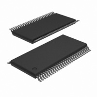
PCA9698DGG/S911,51 NXP Semiconductors, PCA9698DGG/S911,51 Datasheet - Page 30

PCA9698DGG/S911,51
Manufacturer Part Number
PCA9698DGG/S911,51
Description
IC I/O EXPANDER I2C 40B 56TSSOP
Manufacturer
NXP Semiconductors
Datasheet
1.PCA9698BS118.pdf
(48 pages)
Specifications of PCA9698DGG/S911,51
Interface
I²C
Number Of I /o
40
Interrupt Output
Yes
Frequency - Clock
1MHz
Voltage - Supply
2.3 V ~ 5.5 V
Operating Temperature
-40°C ~ 85°C
Mounting Type
Surface Mount
Package / Case
56-TSSOP
Includes
POR
For Use With
OM6281 - DAUGHTER CARD PCA9698 FOR OM6275
Lead Free Status / RoHS Status
Lead free / RoHS Compliant
Other names
935285491518
PCA9698DGG/S911-T
PCA9698DGG/S911-T
PCA9698DGG/S911-T
PCA9698DGG/S911-T
NXP Semiconductors
PCA9698
Product data sheet
Fig 23. GPIO All Call write to the Output Port, I/O Configuration, Polarity Inversion, or Mask interrupt registers
Fig 24. GPIO All Call write to the Output structure configuration, All Bank Control, or Mode selection registers
Only slave devices with bit IOAC = 1 answer to the GPIO All Call transaction.
Output Port register programming becomes effective at the STOP command if OCH = 0, at each acknowledge if OCH = 1.
Configuration, Polarity Inversion, and Mask interrupt registers become effective at the acknowledge.
Less than 5 bytes can be programmed by using the same scheme.
‘D5 D4 D3 D2 D1 D0’ refers to the first register to be programmed.
If more than 5 bytes are written, previous data are overwritten (the sixth Configuration register will roll over to the first
addressed Configuration register, the sixth Polarity Inversion register will roll over to the first addressed Polarity Inversion
register, the sixth Mask interrupt register will roll over to the first addressed Mask interrupt register).
Only slave devices with bit 0 IOAC = 1 answer the GPIO All Call transaction.
The programming becomes effective at the acknowledge.
If more than 1 byte is written, previous data is overwritten.
SDA
S 1
START condition
SDA
GPIO All Call address
1
S 1
START condition
00 for Output structure configuration register programming
01 for All Bank Control register programming
10 for Mode selection register programming
0
1
1
slave address
1
0
acknowledge
1
1
from slave
0 0 A
1
R/W
acknowledge
from slave(s)
All information provided in this document is subject to legal disclaimers.
1
0 0 A
R/W
AI = 1
1
0 D5 D4 D3 D2 D1 D0
40-bit Fm+ I
Rev. 3 — 3 August 2010
command register
AI = 'don't care'
X
0
command register
DATA BANK 2 A
1
0
2
00 1000 for Output Port register programming bank 0
01 0000 for Polarity Inversion register programming bank 0
01 1000 for Configuration register programming bank 0
10 0000 for Mask interrupt register programming bank 0
1
C-bus advanced I/O port with RESET, OE and INT
acknowledge
from slave(s)
0 D1 D0
A
acknowledge
from slave(s)
acknowledge
from slave(s)
DATA BANK 0 A
DATA BANK 3 A
A
acknowledge
from slave(s)
acknowledge
from slave(s)
DATA
DATA BANK 1
DATA BANK 4
acknowledge
from slave(s)
condition
condition
002aab953
STOP
STOP
A
A
A
acknowledge
from slave(s)
acknowledge
from slave
P
PCA9698
P
002aab952
© NXP B.V. 2010. All rights reserved.
30 of 48


