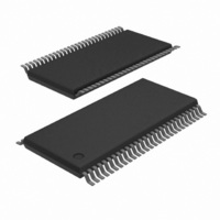
PCA9698DGG/S911,51 NXP Semiconductors, PCA9698DGG/S911,51 Datasheet - Page 14

PCA9698DGG/S911,51
Manufacturer Part Number
PCA9698DGG/S911,51
Description
IC I/O EXPANDER I2C 40B 56TSSOP
Manufacturer
NXP Semiconductors
Datasheet
1.PCA9698BS118.pdf
(48 pages)
Specifications of PCA9698DGG/S911,51
Interface
I²C
Number Of I /o
40
Interrupt Output
Yes
Frequency - Clock
1MHz
Voltage - Supply
2.3 V ~ 5.5 V
Operating Temperature
-40°C ~ 85°C
Mounting Type
Surface Mount
Package / Case
56-TSSOP
Includes
POR
For Use With
OM6281 - DAUGHTER CARD PCA9698 FOR OM6275
Lead Free Status / RoHS Status
Lead free / RoHS Compliant
Other names
935285491518
PCA9698DGG/S911-T
PCA9698DGG/S911-T
PCA9698DGG/S911-T
PCA9698DGG/S911-T
NXP Semiconductors
PCA9698
Product data sheet
7.4.7.1 Examples
7.4.7 ALLBNK - All Bank control register
Table 10.
This register allows all the I/Os configured as outputs to be programmed with the same
logic value. This programming is applied to all the banks or a selection of banks.
When this register is programmed, values in the Output Port registers are not changed
and do not reflect the states of I/Os configured as outputs anymore.
Bit
Symbol
Default
•
•
•
•
•
•
B0 to B4 controls the logic level to be applied to Bank 0 to Bank 4, respectively.
– Bx = 0: All the I/Os configured as outputs in the corresponding Bank x are
– Bx = 1: All the I/Os configured as outputs in the corresponding Bank x are
Bit 5 and bit 6 are not used and can be programmed to either ‘1’ or ‘0’.
BSEL is a filter bit that allows programming of some banks only, and not the others.
– BSEL = 0:
– BSEL = 1:
If ALLBNK = 0XX0 0000:
All I/Os configured as outputs in Bank 0 to Bank 4 will be programmed with 0s,
overwriting values programmed in the five Output Port registers.
If ALLBNK = 1XX1 1111:
All I/Os configured as outputs in Bank 0 to Bank 4 will be programmed with 1s,
overwriting values programmed in the five Output Port registers.
If ALLBNK = 0XX0 0110:
All I/Os configured as outputs in Banks 0, 3, and 4 only will be programmed with 0s,
overwriting values programmed in the Output Port registers 0, 3, and 4, while I/Os
configured as outputs in Bank 1 and Bank 2 are programmed with values in Output
Port registers 1 and 2.
programmed with 0s.
programmed with 1s.
When Bx = 0, all the I/Os configured as output in the corresponding Bank x are
programmed with 0s.
When Bx = 1, all the I/Os configured as output in the corresponding Bank x are
programmed with their actual value from the corresponding output register.
When Bx = 0, all the I/Os configured as output in the corresponding Bank x are
programmed with their actual value from the corresponding output register.
When Bx = 1, all the I/Os configured as output in the corresponding Bank x are
programmed with 1s.
ALLBNK - All Bank control register (address 29h) description
BSEL
7
1
All information provided in this document is subject to legal disclaimers.
40-bit Fm+ I
Rev. 3 — 3 August 2010
X
6
0
X
5
0
2
C-bus advanced I/O port with RESET, OE and INT
B4
4
0
B3
3
0
B2
2
0
PCA9698
© NXP B.V. 2010. All rights reserved.
B1
1
0
14 of 48
B0
0
0


