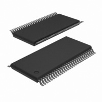
PCA9698DGG/S911,51 NXP Semiconductors, PCA9698DGG/S911,51 Datasheet - Page 24

PCA9698DGG/S911,51
Manufacturer Part Number
PCA9698DGG/S911,51
Description
IC I/O EXPANDER I2C 40B 56TSSOP
Manufacturer
NXP Semiconductors
Datasheet
1.PCA9698BS118.pdf
(48 pages)
Specifications of PCA9698DGG/S911,51
Interface
I²C
Number Of I /o
40
Interrupt Output
Yes
Frequency - Clock
1MHz
Voltage - Supply
2.3 V ~ 5.5 V
Operating Temperature
-40°C ~ 85°C
Mounting Type
Surface Mount
Package / Case
56-TSSOP
Includes
POR
For Use With
OM6281 - DAUGHTER CARD PCA9698 FOR OM6275
Lead Free Status / RoHS Status
Lead free / RoHS Compliant
Other names
935285491518
PCA9698DGG/S911-T
PCA9698DGG/S911-T
PCA9698DGG/S911-T
PCA9698DGG/S911-T
NXP Semiconductors
PCA9698
Product data sheet
Fig 13. System configuration
SDA
SCL
TRANSMITTER/
RECEIVER
MASTER
8.2 System configuration
8.3 Acknowledge
A device generating a message is a ‘transmitter’; a device receiving is the ‘receiver’. The
device that controls the message is the ‘master’ and the devices which are controlled by
the master are the ‘slaves’ (see
The number of data bytes transferred between the START and the STOP conditions from
transmitter to receiver is not limited. Each byte of eight bits is followed by one
acknowledge bit. The acknowledge bit is a HIGH level put on the bus by the transmitter,
whereas the master generates an extra acknowledge related clock pulse.
A slave receiver which is addressed must generate an acknowledge after the reception of
each byte. Also a master must generate an acknowledge after the reception of each byte
that has been clocked out of the slave transmitter. The device that acknowledges has to
pull down the SDA line during the acknowledge clock pulse, so that the SDA line is stable
LOW during the HIGH period of the acknowledge related clock pulse; set-up and hold
times must be taken into account.
A master receiver must signal an end of data to the transmitter by not generating an
acknowledge on the last byte that has been clocked out of the slave. In this event, the
transmitter must leave the data line HIGH to enable the master to generate a STOP
condition.
Fig 14. Acknowledgement on the I
RECEIVER
SLAVE
SCL from master
by transmitter
data output
data output
by receiver
All information provided in this document is subject to legal disclaimers.
TRANSMITTER/
40-bit Fm+ I
Rev. 3 — 3 August 2010
RECEIVER
condition
START
SLAVE
S
Figure
2
2
C-bus
C-bus advanced I/O port with RESET, OE and INT
TRANSMITTER
1
13).
MASTER
2
TRANSMITTER/
RECEIVER
MASTER
acknowledgement
not acknowledge
SLAVE
clock pulse for
acknowledge
8
MULTIPLEXER
PCA9698
© NXP B.V. 2010. All rights reserved.
002aaa987
I
2
9
C-BUS
002aaa966
24 of 48


