A000003 Arduino, A000003 Datasheet - Page 238
A000003
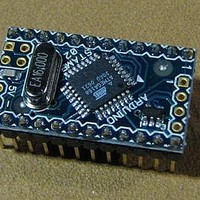
Manufacturer Part Number
A000003
Description
MCU, MPU & DSP Development Tools MINI
Manufacturer
Arduino
Series
-r
Type
MCUr
Specifications of A000003
Processor To Be Evaluated
Atmega328
Processor Series
ATmega
Data Bus Width
8 bit
Interface Type
USB, RS-232
Operating Supply Voltage
7 V to 9 V
Contents
Board
Lead Free Status / Rohs Status
Lead free / RoHS Compliant
For Use With/related Products
ATmega168


21.9.5
21.9.6
238
ATmega48/88/168
TWAR – TWI (Slave) Address Register
TWAMR – TWI (Slave) Address Mask Register
of a lost bus arbitration, no data is lost in the transition from Master to Slave. Handling of the
ACK bit is controlled automatically by the TWI logic, the CPU cannot access the ACK bit directly.
• Bits 7..0 – TWD: TWI Data Register
These eight bits constitute the next data byte to be transmitted, or the latest data byte received
on the 2-wire Serial Bus.
The TWAR should be loaded with the 7-bit Slave address (in the seven most significant bits of
TWAR) to which the TWI will respond when programmed as a Slave Transmitter or Receiver,
and not needed in the Master modes. In multi master systems, TWAR must be set in masters
which can be addressed as Slaves by other Masters.
The LSB of TWAR is used to enable recognition of the general call address (0x00). There is an
associated address comparator that looks for the slave address (or general call address if
enabled) in the received serial address. If a match is found, an interrupt request is generated.
• Bits 7..1 – TWA: TWI (Slave) Address Register
These seven bits constitute the slave address of the TWI unit.
• Bit 0 – TWGCE: TWI General Call Recognition Enable Bit
If set, this bit enables the recognition of a General Call given over the 2-wire Serial Bus.
• Bits 7..1 – TWAM: TWI Address Mask
The TWAMR can be loaded with a 7-bit Salve Address mask. Each of the bits in TWAMR can
mask (disable) the corresponding address bits in the TWI Address Register (TWAR). If the mask
bit is set to one then the address match logic ignores the compare between the incoming
address bit and the corresponding bit in TWAR.
detail.
Bit
(0xBA)
Read/Write
Initial Value
Bit
(0xBD)
Read/Write
Initial Value
TWA6
R/W
R/W
7
1
7
0
TWA5
R/W
R/W
6
1
6
0
TWA4
R/W
R/W
5
0
5
1
TWAM[6:0]
TWA3
R/W
R/W
4
1
4
0
Figure 21-22
TWA2
R/W
R/W
3
0
3
1
TWA1
R/W
R/W
shown the address match logic in
2
0
2
1
TWA0
R/W
R/W
1
0
1
1
TWGCE
R/W
R
0
–
0
0
0
2545S–AVR–07/10
TWAMR
TWAR
Related parts for A000003
Image
Part Number
Description
Manufacturer
Datasheet
Request
R

Part Number:
Description:
Daughter Cards & OEM Boards ARDUINO UNO PROTO PCB REV 3
Manufacturer:
Arduino
Part Number:
Description:
Daughter Cards & OEM Boards ARDUINO SHIELD PROTO KIT REV 3
Manufacturer:
Arduino
Part Number:
Description:
Daughter Cards & OEM Boards ARDUINO MEGA PROTO KIT REV 3
Manufacturer:
Arduino
Part Number:
Description:
Daughter Cards & OEM Boards ARDUINO MEGA PROTO PCB REV 3
Manufacturer:
Arduino
Part Number:
Description:
Development Boards & Kits - AVR ARDUINO STARTER KIT W/ UNO REV3
Manufacturer:
Arduino
Part Number:
Description:
RF Development Tools ARDUINO SHIELD WIRELESS PROTO
Manufacturer:
Arduino
Datasheet:
Part Number:
Description:
RF Development Tools ARDUINO SHIELD WIRELESS WITH SD
Manufacturer:
Arduino
Datasheet:

Part Number:
Description:
Development Software Getting started w/Arduino
Manufacturer:
Arduino

Part Number:
Description:
Ethernet Modules & Development Tools Ethernet Shield for Arduino
Manufacturer:
Arduino

Part Number:
Description:
MCU, MPU & DSP Development Tools LilyPad Arduino Main Board
Manufacturer:
Arduino

Part Number:
Description:
ARDUINO NANO Board
Manufacturer:
Arduino
Datasheet:
Part Number:
Description:
Ethernet Modules & Development Tools ETHERNET SHEILD PoE FOR ARDUINO
Manufacturer:
Arduino
Datasheet:

Part Number:
Description:
ATMEGA328 MCU IC W/ Arduino UNO Bootloader
Manufacturer:
Arduino
Datasheet:
Part Number:
Description:
Memory Cards MICRO SD CARD 1GB WITH SD ADAPTER
Manufacturer:
Arduino