A000003 Arduino, A000003 Datasheet - Page 155
A000003
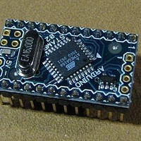
Manufacturer Part Number
A000003
Description
MCU, MPU & DSP Development Tools MINI
Manufacturer
Arduino
Series
-r
Type
MCUr
Specifications of A000003
Processor To Be Evaluated
Atmega328
Processor Series
ATmega
Data Bus Width
8 bit
Interface Type
USB, RS-232
Operating Supply Voltage
7 V to 9 V
Contents
Board
Lead Free Status / Rohs Status
Lead free / RoHS Compliant
For Use With/related Products
ATmega168


17.11.2
2545S–AVR–07/10
TCCR2B – Timer/Counter Control Register B
Table 17-8.
Notes:
• Bit 7 – FOC2A: Force Output Compare A
The FOC2A bit is only active when the WGM bits specify a non-PWM mode.
However, for ensuring compatibility with future devices, this bit must be set to zero when
TCCR2B is written when operating in PWM mode. When writing a logical one to the FOC2A bit,
an immediate Compare Match is forced on the Waveform Generation unit. The OC2A output is
changed according to its COM2A1:0 bits setting. Note that the FOC2A bit is implemented as a
strobe. Therefore it is the value present in the COM2A1:0 bits that determines the effect of the
forced compare.
A FOC2A strobe will not generate any interrupt, nor will it clear the timer in CTC mode using
OCR2A as TOP.
The FOC2A bit is always read as zero.
• Bit 6 – FOC2B: Force Output Compare B
The FOC2B bit is only active when the WGM bits specify a non-PWM mode.
However, for ensuring compatibility with future devices, this bit must be set to zero when
TCCR2B is written when operating in PWM mode. When writing a logical one to the FOC2B bit,
an immediate Compare Match is forced on the Waveform Generation unit. The OC2B output is
changed according to its COM2B1:0 bits setting. Note that the FOC2B bit is implemented as a
strobe. Therefore it is the value present in the COM2B1:0 bits that determines the effect of the
forced compare.
Bit
(0xB1)
Read/Write
Initial Value
Mode
0
1
2
3
4
5
6
7
1. MAX= 0xFF
2. BOTTOM= 0x00
WGM2
0
0
0
0
1
1
1
1
Waveform Generation Mode Bit Description
FOC2A
W
7
0
WGM1
0
0
1
1
0
0
1
1
FOC2B
W
6
0
WGM0
0
1
0
1
0
1
0
1
R
5
–
0
Timer/Counter
Mode of
Operation
Normal
PWM, Phase
Correct
CTC
Fast PWM
Reserved
PWM, Phase
Correct
Reserved
Fast PWM
R
4
–
0
WGM22
R
3
0
OCRA
OCRA
OCRA
0xFF
0xFF
0xFF
TOP
ATmega48/88/168
CS22
–
–
R
2
0
Immediate
Immediate
Update of
BOTTOM
BOTTOM
OCRx at
CS21
R/W
1
0
TOP
TOP
–
–
CS20
R/W
0
0
Set on
TOV Flag
BOTTOM
BOTTOM
MAX
MAX
MAX
TOP
TCCR2B
–
–
(1)(2)
155
Related parts for A000003
Image
Part Number
Description
Manufacturer
Datasheet
Request
R

Part Number:
Description:
Daughter Cards & OEM Boards ARDUINO UNO PROTO PCB REV 3
Manufacturer:
Arduino
Part Number:
Description:
Daughter Cards & OEM Boards ARDUINO SHIELD PROTO KIT REV 3
Manufacturer:
Arduino
Part Number:
Description:
Daughter Cards & OEM Boards ARDUINO MEGA PROTO KIT REV 3
Manufacturer:
Arduino
Part Number:
Description:
Daughter Cards & OEM Boards ARDUINO MEGA PROTO PCB REV 3
Manufacturer:
Arduino
Part Number:
Description:
Development Boards & Kits - AVR ARDUINO STARTER KIT W/ UNO REV3
Manufacturer:
Arduino
Part Number:
Description:
RF Development Tools ARDUINO SHIELD WIRELESS PROTO
Manufacturer:
Arduino
Datasheet:
Part Number:
Description:
RF Development Tools ARDUINO SHIELD WIRELESS WITH SD
Manufacturer:
Arduino
Datasheet:

Part Number:
Description:
Development Software Getting started w/Arduino
Manufacturer:
Arduino

Part Number:
Description:
Ethernet Modules & Development Tools Ethernet Shield for Arduino
Manufacturer:
Arduino

Part Number:
Description:
MCU, MPU & DSP Development Tools LilyPad Arduino Main Board
Manufacturer:
Arduino

Part Number:
Description:
ARDUINO NANO Board
Manufacturer:
Arduino
Datasheet:
Part Number:
Description:
Ethernet Modules & Development Tools ETHERNET SHEILD PoE FOR ARDUINO
Manufacturer:
Arduino
Datasheet:

Part Number:
Description:
ATMEGA328 MCU IC W/ Arduino UNO Bootloader
Manufacturer:
Arduino
Datasheet:
Part Number:
Description:
Memory Cards MICRO SD CARD 1GB WITH SD ADAPTER
Manufacturer:
Arduino