A000003 Arduino, A000003 Datasheet - Page 142
A000003
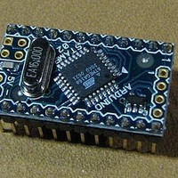
Manufacturer Part Number
A000003
Description
MCU, MPU & DSP Development Tools MINI
Manufacturer
Arduino
Series
-r
Type
MCUr
Specifications of A000003
Processor To Be Evaluated
Atmega328
Processor Series
ATmega
Data Bus Width
8 bit
Interface Type
USB, RS-232
Operating Supply Voltage
7 V to 9 V
Contents
Board
Lead Free Status / Rohs Status
Lead free / RoHS Compliant
For Use With/related Products
ATmega168


17.5.1
17.5.2
17.5.3
142
ATmega48/88/168
Force Output Compare
Compare Match Blocking by TCNT2 Write
Using the Output Compare Unit
Figure 17-3. Output Compare Unit, Block Diagram
The OCR2x Register is double buffered when using any of the Pulse Width Modulation (PWM)
modes. For the Normal and Clear Timer on Compare (CTC) modes of operation, the double
buffering is disabled. The double buffering synchronizes the update of the OCR2x Compare
Register to either top or bottom of the counting sequence. The synchronization prevents the
occurrence of odd-length, non-symmetrical PWM pulses, thereby making the output glitch-free.
The OCR2x Register access may seem complex, but this is not case. When the double buffering
is enabled, the CPU has access to the OCR2x Buffer Register, and if double buffering is dis-
abled the CPU will access the OCR2x directly.
In non-PWM waveform generation modes, the match output of the comparator can be forced by
writing a one to the Force Output Compare (FOC2x) bit. Forcing compare match will not set the
OCF2x Flag or reload/clear the timer, but the OC2x pin will be updated as if a real compare
match had occurred (the COM2x1:0 bits settings define whether the OC2x pin is set, cleared or
toggled).
All CPU write operations to the TCNT2 Register will block any compare match that occurs in the
next timer clock cycle, even when the timer is stopped. This feature allows OCR2x to be initial-
ized to the same value as TCNT2 without triggering an interrupt when the Timer/Counter clock is
enabled.
Since writing TCNT2 in any mode of operation will block all compare matches for one timer clock
cycle, there are risks involved when changing TCNT2 when using the Output Compare channel,
independently of whether the Timer/Counter is running or not. If the value written to TCNT2
equals the OCR2x value, the compare match will be missed, resulting in incorrect waveform
generation. Similarly, do not write the TCNT2 value equal to BOTTOM when the counter is
downcounting.
bottom
FOCn
top
OCRnx
Waveform Generator
WGMn1:0
=
(8-bit Comparator )
DATA BUS
COMnX1:0
TCNTn
OCFnx (Int.Req.)
OCnx
2545S–AVR–07/10
Related parts for A000003
Image
Part Number
Description
Manufacturer
Datasheet
Request
R

Part Number:
Description:
Daughter Cards & OEM Boards ARDUINO UNO PROTO PCB REV 3
Manufacturer:
Arduino
Part Number:
Description:
Daughter Cards & OEM Boards ARDUINO SHIELD PROTO KIT REV 3
Manufacturer:
Arduino
Part Number:
Description:
Daughter Cards & OEM Boards ARDUINO MEGA PROTO KIT REV 3
Manufacturer:
Arduino
Part Number:
Description:
Daughter Cards & OEM Boards ARDUINO MEGA PROTO PCB REV 3
Manufacturer:
Arduino
Part Number:
Description:
Development Boards & Kits - AVR ARDUINO STARTER KIT W/ UNO REV3
Manufacturer:
Arduino
Part Number:
Description:
RF Development Tools ARDUINO SHIELD WIRELESS PROTO
Manufacturer:
Arduino
Datasheet:
Part Number:
Description:
RF Development Tools ARDUINO SHIELD WIRELESS WITH SD
Manufacturer:
Arduino
Datasheet:

Part Number:
Description:
Development Software Getting started w/Arduino
Manufacturer:
Arduino

Part Number:
Description:
Ethernet Modules & Development Tools Ethernet Shield for Arduino
Manufacturer:
Arduino

Part Number:
Description:
MCU, MPU & DSP Development Tools LilyPad Arduino Main Board
Manufacturer:
Arduino

Part Number:
Description:
ARDUINO NANO Board
Manufacturer:
Arduino
Datasheet:
Part Number:
Description:
Ethernet Modules & Development Tools ETHERNET SHEILD PoE FOR ARDUINO
Manufacturer:
Arduino
Datasheet:

Part Number:
Description:
ATMEGA328 MCU IC W/ Arduino UNO Bootloader
Manufacturer:
Arduino
Datasheet:
Part Number:
Description:
Memory Cards MICRO SD CARD 1GB WITH SD ADAPTER
Manufacturer:
Arduino