A000003 Arduino, A000003 Datasheet - Page 171
A000003
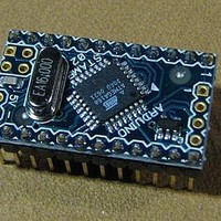
Manufacturer Part Number
A000003
Description
MCU, MPU & DSP Development Tools MINI
Manufacturer
Arduino
Series
-r
Type
MCUr
Specifications of A000003
Processor To Be Evaluated
Atmega328
Processor Series
ATmega
Data Bus Width
8 bit
Interface Type
USB, RS-232
Operating Supply Voltage
7 V to 9 V
Contents
Board
Lead Free Status / Rohs Status
Lead free / RoHS Compliant
For Use With/related Products
ATmega168


19.3
2545S–AVR–07/10
Clock Generation
Figure 19-1. USART Block Diagram
Note:
The Clock Generation logic generates the base clock for the Transmitter and Receiver. The
USART supports four modes of clock operation: Normal asynchronous, Double Speed asyn-
chronous, Master synchronous and Slave synchronous mode. The UMSELn bit in USART
Control and Status Register C (UCSRnC) selects between asynchronous and synchronous
operation. Double Speed (asynchronous mode only) is controlled by the U2Xn found in the
UCSRnA Register. When using synchronous mode (UMSELn = 1), the Data Direction Register
for the XCKn pin (DDR_XCKn) controls whether the clock source is internal (Master mode) or
external (Slave mode). The XCKn pin is only active when using synchronous mode.
Figure 19-2
1. Refer to
shows a block diagram of the clock generation logic.
Figure 1-1 on page 2
UCSRnA
TRANSMIT SHIFT REGISTER
RECEIVE SHIFT REGISTER
BAUD RATE GENERATOR
UDRn (Receive)
UDRn(Transmit)
UBRRn [H:L]
(1)
and
Table 13-9 on page 83
UCSRnB
GENERATOR
SYNC LOGIC
RECOVERY
RECOVERY
CHECKER
PARITY
PARITY
CLOCK
DATA
OSC
ATmega48/88/168
for USART0 pin placement.
Clock Generator
CONTROL
CONTROL
CONTROL
CONTROL
CONTROL
Transmitter
PIN
PIN
PIN
RX
TX
Receiver
UCSRnC
XCKn
TxDn
RxDn
171
Related parts for A000003
Image
Part Number
Description
Manufacturer
Datasheet
Request
R

Part Number:
Description:
Daughter Cards & OEM Boards ARDUINO UNO PROTO PCB REV 3
Manufacturer:
Arduino
Part Number:
Description:
Daughter Cards & OEM Boards ARDUINO SHIELD PROTO KIT REV 3
Manufacturer:
Arduino
Part Number:
Description:
Daughter Cards & OEM Boards ARDUINO MEGA PROTO KIT REV 3
Manufacturer:
Arduino
Part Number:
Description:
Daughter Cards & OEM Boards ARDUINO MEGA PROTO PCB REV 3
Manufacturer:
Arduino
Part Number:
Description:
Development Boards & Kits - AVR ARDUINO STARTER KIT W/ UNO REV3
Manufacturer:
Arduino
Part Number:
Description:
RF Development Tools ARDUINO SHIELD WIRELESS PROTO
Manufacturer:
Arduino
Datasheet:
Part Number:
Description:
RF Development Tools ARDUINO SHIELD WIRELESS WITH SD
Manufacturer:
Arduino
Datasheet:

Part Number:
Description:
Development Software Getting started w/Arduino
Manufacturer:
Arduino

Part Number:
Description:
Ethernet Modules & Development Tools Ethernet Shield for Arduino
Manufacturer:
Arduino

Part Number:
Description:
MCU, MPU & DSP Development Tools LilyPad Arduino Main Board
Manufacturer:
Arduino

Part Number:
Description:
ARDUINO NANO Board
Manufacturer:
Arduino
Datasheet:
Part Number:
Description:
Ethernet Modules & Development Tools ETHERNET SHEILD PoE FOR ARDUINO
Manufacturer:
Arduino
Datasheet:

Part Number:
Description:
ATMEGA328 MCU IC W/ Arduino UNO Bootloader
Manufacturer:
Arduino
Datasheet:
Part Number:
Description:
Memory Cards MICRO SD CARD 1GB WITH SD ADAPTER
Manufacturer:
Arduino