VSC8211XVW Vitesse Semiconductor Corp, VSC8211XVW Datasheet - Page 29
VSC8211XVW
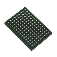
Manufacturer Part Number
VSC8211XVW
Description
IC PHY 10/100/1000 SGL 117-LBGA
Manufacturer
Vitesse Semiconductor Corp
Type
PHY Transceiverr
Specifications of VSC8211XVW
Number Of Drivers/receivers
1/1
Protocol
Gigabit Ethernet
Voltage - Supply
3 V ~ 3.6 V
Mounting Type
Surface Mount
Package / Case
117-LBGA
Case
BGA
Dc
07+
Lead Free Status / RoHS Status
Lead free / RoHS Compliant
Other names
907-1023
Available stocks
Company
Part Number
Manufacturer
Quantity
Price
Company:

Part Number:
VSC8211XVW
Manufacturer:
VITESSE
Quantity:
5
Company:
Part Number:
VSC8211XVW
Manufacturer:
Semtech
Quantity:
3 413
Company:
Part Number:
VSC8211XVW
Manufacturer:
VITESSE
Quantity:
648
Company:
Part Number:
VSC8211XVW
Manufacturer:
Vitesse Semiconductor Corporation
Quantity:
10 000
Part Number:
VSC8211XVW
Manufacturer:
VITESSE
Quantity:
20 000


VMDS-10105 Revision 4.1
October 2006
LBGA
BALL
117
A3
A5
A4
PMARX
CLK1
RX[8]
RX[9]
TBI
Parallel MAC Interface Modes
uncon-
nected
uncon-
nected
Leave
Leave
RD[9]
RD[4]
RTBI
pins
pins
and
Table 10. Parallel MAC Interface Signals - Receive Signals (continued)
Signal Name
uncon-
nected
RXDV
RXER
Leave
GMII
pins
TXCLK
RXDV
RXER
MII
RXCTL OZC
uncon-
uncon-
RGMII
nected
nected
Leave
Leave
pins
pins
Type
O
O
29 of 165
ZC
ZC
PMA Receiver Clock 1 Output (TBI mode).
The protocol device (MAC) uses the rising edge of this
62.5MHz receive clock to latch even-numbered code groups
on the received PHY bit stream. PMARXCLK1 is 180
phase with PMARXCLK0. This clock may be stretched during
code-group alignment and is not shortened.
Transmit Clock (MII mode).
25MHz (100Mb mode) or 2.5MHz (10Mb mode) MII clock out-
put. The MAC uses the rising edge of this clock to synchro-
nize TXD data.
Receive Data Code Group, bit [8] (TBI mode).
Bit [8] of 10-bit parallel receive code-group data. When code
groups are properly aligned, any received code group con-
taining a comma is clocked by the rising edge of
PMARXCLK1.
Receive Data Valid Output (GMII, MII modes).
RXDV is asserted by the PHY to indicate that the PHY is pre-
senting recovered and decoded data on the RXD pins. RXDV
is synchronous with respect to RXCLK.
Receive Data Code Group, bit [9] (TBI mode).
Bit [9] of 10-bit parallel receive code-group data. When code
groups are properly aligned, any received code group con-
taining a comma is clocked by the rising edge of
PMARXCLK1.
Multiplexed Receive Data Nibbles (RTBI mode).
The MAC synchronously inputs Bit [4] on the rising edge of
RXC, and bit [9] (MSB) on the falling edge of RXC.
Receiver Error Output (GMII, MII modes).
This active high output is synchronous to the rising edge of
the received data clock (RXCLK or RXC). For 1000Mb mode,
this signal is asserted when error symbols or carrier exten-
sion symbols are received. In 100Mb mode, it is asserted
when error symbols are received.
Multiplexed Receive Data Valid / Receive Error Output
(RGMII mode).
In RGMII mode, this output is sampled by the MAC on oppo-
site edges of RXC to indicate two receive conditions from the
PHY:
1) on the rising edge of RXC, this output serves as RXDV.
When high it signals valid data is available on the RD input
data bus.
2) on the falling edge of RXC, this output signals a receive
error from the PHY, based on a logical derivative of RXDV
and RXER, per RGMII specification Version 1.2a, Section 3.4.
Description
Datasheet
VSC8211
o
out of
Related parts for VSC8211XVW
Image
Part Number
Description
Manufacturer
Datasheet
Request
R

Part Number:
Description:
Single Port 10/100/1000base-t Phy And 1000base-x Phy With Sgmii, Serdes, Gmii, Mii, Tbi, Rgmii / Rtbi Mac Interfaces Semiconductor Corporation
Manufacturer:
Vitesse Semiconductor Corp
Datasheet:
Part Number:
Description:
Multi-rate 16 1 Sonet/sdh Transceiver With Integrated Clock Generator Semiconductor Corporation
Manufacturer:
Vitesse Semiconductor Corp
Datasheet:
Part Number:
Description:
2.488gb/s 4 1 Sonet/sdh Transceiver With Integrated Clock Generator Semiconductor Corporation
Manufacturer:
Vitesse Semiconductor Corp
Datasheet:
Part Number:
Description:
2.488 Gbit/sec To 2.7gbit/sec 1 16 Sonet/sdh Demux Semiconductor Corporation
Manufacturer:
Vitesse Semiconductor Corp
Datasheet:
Part Number:
Description:
10.3125 Gbps Advanced Electronic Equalization With Limiting Amplifier, And Clock And Data Recovery Semiconductor Corporation
Manufacturer:
Vitesse Semiconductor Corp
Datasheet:
Part Number:
Description:
34x34 Crosspoint Switch With Signal Detection Semiconductor Corporation
Manufacturer:
Vitesse Semiconductor Corp
Datasheet:
Part Number:
Description:
10 Gbps Queue Manager With Integrated Spi4.2 Interface Semiconductor Corporation
Manufacturer:
Vitesse Semiconductor Corp
Datasheet:
Part Number:
Description:
High Performance 16x16 Serial Crosspoint Switch Semiconductor Corporation
Manufacturer:
Vitesse Semiconductor Corp
Datasheet:
Part Number:
Description:
16-port Jbod Loop Chip For 1.0625 Gb/s Fc-al Storage Applications Semiconductor Corporation
Manufacturer:
Vitesse Semiconductor Corp
Datasheet:
Part Number:
Description:
Quad Port Bypass Circuit Semiconductor Corporation
Manufacturer:
Vitesse Semiconductor Corp
Datasheet:

Part Number:
Description:
IC PHY 10/100/1000 64-EP-LQFP
Manufacturer:
Vitesse Semiconductor Corp
Datasheet:

Part Number:
Description:
IC PHY 10/100/1000 260-HS-PBGA
Manufacturer:
Vitesse Semiconductor Corp
Datasheet:

Part Number:
Description:
IC PHY 10/100/1000 444-HS-BGA
Manufacturer:
Vitesse Semiconductor Corp
Datasheet:

Part Number:
Description:
IC TXRX MULTIRATE 16BIT 208-BGA
Manufacturer:
Vitesse Semiconductor Corp
Datasheet:
Part Number:
Description:
TRANSCEIVER SRL XAUI XGMII I/O
Manufacturer:
Vitesse Semiconductor Corp