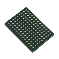
VSC8211XVW Vitesse Semiconductor Corp, VSC8211XVW Datasheet - Page 150

VSC8211XVW
Manufacturer Part Number
VSC8211XVW
Description
IC PHY 10/100/1000 SGL 117-LBGA
Manufacturer
Vitesse Semiconductor Corp
Type
PHY Transceiverr
Specifications of VSC8211XVW
Number Of Drivers/receivers
1/1
Protocol
Gigabit Ethernet
Voltage - Supply
3 V ~ 3.6 V
Mounting Type
Surface Mount
Package / Case
117-LBGA
Case
BGA
Dc
07+
Lead Free Status / RoHS Status
Lead free / RoHS Compliant
Other names
907-1023
Available stocks
Company
Part Number
Manufacturer
Quantity
Price
Company:
Part Number:
VSC8211XVW
Manufacturer:
VITESSE
Quantity:
5
Company:
Part Number:
VSC8211XVW
Manufacturer:
Semtech
Quantity:
3 413
Company:
Part Number:
VSC8211XVW
Manufacturer:
VITESSE
Quantity:
648
Company:
Part Number:
VSC8211XVW
Manufacturer:
Vitesse Semiconductor Corporation
Quantity:
10 000
Part Number:
VSC8211XVW
Manufacturer:
VITESSE
Quantity:
20 000
1
2
3
30.7 RGMII/RTBI Mode Timing
For RGMII/RTBI modes, the following specifications are valid when the I/O power supply (VDDIOMAC) is 2.5V or 3.3V, ±5%,
per the RGMII v2.0 specification, and the MAC/Media Interface Mode Select bits (see
Extended PHY Control Register #4,”
VMDS-10105 Revision 4.1
October 2006
This implies that PC board design will require clocks to be routed such that an additional trace delay of greater than 1.5ns and less than 2.0ns will be added to the
associated clock signal. This is normal operating mode (RGMII timing is not compensated). To enable RGMII timing compensation, see
RGMII-ID mode (RGMII with Internal Delay Compensation On) - a programmable delay of 0ns, 1.5ns, 2.0ns, or 2.5ns is added to the TXC and RXC signals inside
the PHY. Each of delays is independently programmable using
Duty cycle may be stretched or shrunk during speed changes or while transitioning to a received packet’s clock domain, as long as the minimum duty cycle is not
violated, and stretching occurs for no more than three T
Duty
Symbol
T
V
V
V
Duty
T
T
T
T
T
T
T
CYC1000
T
T
thresh1.5
thresh2.5
thresh3.3
CYC100
setup
skew
setup
CYC10
skew
hold
hold
R,
10/100
1000
T
R
T
R
T
T
R
F
Min
-500
360
1.2
1.2
1.0
1.0
7.2
36
45
40
1
page 129) have been set to RGMII/RTBI mode.
Typ
0.75
1.25
1.65
400
1.8
2.0
2.0
2.0
2.0
40
50
50
0
8
CYC
Table 66. RGMII/RTBI Mode Timing
of the lowest speed transitioned between.
MII register
Max
500
440
2.6
8.8
.75
44
55
60
0
0
0
0
150 of 165
23.11:8.
Unit
ps
ns
ns
ns
ns
ns
ns
ns
%
%
V
V
V
Data to clock output skew (at PHY) – uncompensated
mode
Data to clock output skew (at receiver) –
uncompensated mode
Data to clock output Setup (at PHY integrated delay)
Data to clock output Setup (at transmitter integrated
delay)
Data to clock output Setup (at receiver integrated
delay)
Data to clock output Setup (at PHY integrated delay)
Clock cycle duration
Duty cycle for 1000BASE-T
Duty cycle for 10BASE-T and 100BASE-TX
Rise, fall time (20% to 80%)
TXCLK Switching Threshold based on VDDIOMAC
Parameter Description & Conditions
2
2
section 25.4.8 “Register 23E (17h) -
1
3
MII Register
Datasheet
VSC8211
3
23.11:8.
2
2


