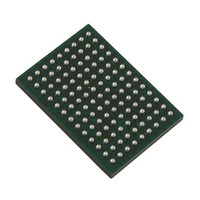
VSC8211XVW Vitesse Semiconductor Corp, VSC8211XVW Datasheet - Page 22

VSC8211XVW
Manufacturer Part Number
VSC8211XVW
Description
IC PHY 10/100/1000 SGL 117-LBGA
Manufacturer
Vitesse Semiconductor Corp
Type
PHY Transceiverr
Specifications of VSC8211XVW
Number Of Drivers/receivers
1/1
Protocol
Gigabit Ethernet
Voltage - Supply
3 V ~ 3.6 V
Mounting Type
Surface Mount
Package / Case
117-LBGA
Case
BGA
Dc
07+
Lead Free Status / RoHS Status
Lead free / RoHS Compliant
Other names
907-1023
Available stocks
Company
Part Number
Manufacturer
Quantity
Price
Company:
Part Number:
VSC8211XVW
Manufacturer:
VITESSE
Quantity:
5
Company:
Part Number:
VSC8211XVW
Manufacturer:
Semtech
Quantity:
3 413
Company:
Part Number:
VSC8211XVW
Manufacturer:
VITESSE
Quantity:
648
Company:
Part Number:
VSC8211XVW
Manufacturer:
Vitesse Semiconductor Corporation
Quantity:
10 000
Part Number:
VSC8211XVW
Manufacturer:
VITESSE
Quantity:
20 000
9.4.2 System Clock Interface Signals (SCI)
VMDS-10105 Revision 4.1
October 2006
117 LBGA
BALL
H10
A10
J10
G6
CLKOUTMICRO/
CLKOUTMAC
Signal Name
MODDEF0/
REFCLK
OSCDIS
XTAL1/
XTAL2
I
Type
PU
O
O
I
/O
Table 3. System Clock Interface Signals (SCI)
XTAL1 - Crystal Oscillator Input.
Enabled by pulling
resonant crystal, with a +/- 50ppm frequency tolerance, should be connected
across XTAL1 and XTAL2. 33pF capacitors should be connected from XTAL1 and
XTAL2 to ground. PLLMODE should be left floating (or pulled low) on reset when a
25MHz crystal is used.
REFCLK - PHY Reference Clock Input.
The reference input clock can either be a 25MHz (PLLMODE is low) or 125MHz
(PLLMODE is high) reference clock, with a +/-50ppm frequency tolerance. See
EECLK / PLLMODE
Crystal Output.
25MHz parallel resonant crystal oscillator output. 33pF capacitors should be con-
nected from both XTAL1 and XTAL2 to ground when using a crystal.
should be left floating (or tied low) on reset when using the 25MHz crystal.
This output can be left floating if driving XTAL1/REFCLK with a reference clock.
CLKOUTMICRO - Clock Output.
This is a 4MHz (default) or a 125MHz output clock depending on the value of
Extended
hardware configuration. Refer to
CMODE Pins”
OMICRO power supply.
OSCDIS - Active Low on-chip Oscillator Disable Input.
This input is sampled during the device power-up sequence or on assertion of
RESET. When sampled high, the PHY enables the internal on-chip oscillator
allowing operation with a 25MHz crystal. When sampled low, the PHY’s oscillator
is turned off and the PHY must be supplied with an external 25MHz or 125MHz
clock on the REFCLK pin.
The functionality of this signal pin depends on the value for Extended
21E.15 ‘SFP Mode’
uration Using CMODE Pins”
configuration at startup.
MODDEF0 – Active Low PHY Ready Indicator Output (valid in SFP Mode,
when
This output is driven high immediately on PHY power-up or reset. This signal is
asserted low after the PHY startup sequence has completed and the PHY has
enabled access to the EEPROM connected to EEPROM Interface through the
Serial Management Interface. The minimum time this signal is high before being
driven low is 10ms. The maximum time depends on the startup information stored
in the EEPROM. Refer to
Section 20: “EEPROM Interface”
CLKOUTMAC – 125MHz Clock Output (valid in IEEE Mode, when
21E.15
The PHY drive a 125MHz clock output after the PHY startup sequence has com-
pleted. This clock can be disabled by clearing
MII Register 21E.15
= 0).
MII Register
22 of 165
for details. The voltage levels of the clock are based on the VDDI-
OSCDIS
which is set at startup. Refer to
pin description for more details.
20E.8. The clock output frequency can be set at startup by
Section 21: “PHY Startup and Initialization”
= 1).
(Internal Oscillator Disabled) high, a 25MHz parallel
and
Section 19: “Hardware Configuration Using
Section 20: “EEPROM Interface”
for details.
Description
MII Register
Section 19: “Hardware Config-
18.0.
for details on
MII Register
PLLMODE
MII Register
and
Datasheet
VSC8211


