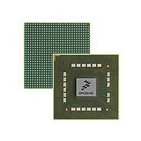
MPC8544VTALF Freescale Semiconductor, MPC8544VTALF Datasheet - Page 66

MPC8544VTALF
Manufacturer Part Number
MPC8544VTALF
Description
MPU POWERQUICC III 783-PBGA
Manufacturer
Freescale Semiconductor
Datasheets
1.MPC8544VTALF.pdf
(117 pages)
2.MPC8544VTALF.pdf
(2 pages)
3.MPC8544VTALF.pdf
(1340 pages)
Specifications of MPC8544VTALF
Processor Type
MPC85xx PowerQUICC III 32-Bit
Speed
667MHz
Voltage
1V
Mounting Type
Surface Mount
Package / Case
783-FCPBGA
Processor Series
MPC85xx
Core
e500
Data Bus Width
32 bit
Maximum Clock Frequency
667 MHz
Maximum Operating Temperature
+ 105 C
Mounting Style
SMD/SMT
Data Ram Size
32 KB
I/o Voltage
1.8 V, 3.3 V
Interface Type
I2C, HSSI, DUART
Minimum Operating Temperature
0 C
Lead Free Status / RoHS Status
Lead free / RoHS Compliant
Features
-
Lead Free Status / Rohs Status
Lead free / RoHS Compliant
Available stocks
Company
Part Number
Manufacturer
Quantity
Price
Company:
Part Number:
MPC8544VTALF
Manufacturer:
Freescale Semiconductor
Quantity:
10 000
Company:
Part Number:
MPC8544VTALFA
Manufacturer:
Freescale Semiconductor
Quantity:
10 000
High-Speed Serial Interfaces (HSSI)
16.2.2
The DC level requirement for the MPC8544E SerDes reference clock inputs is different depending on the
signaling mode used to connect the clock driver chip and SerDes reference clock inputs as described
below.
66
•
•
•
— The SerDes reference clock input can be either differential or single-ended. Refer to the
The maximum average current requirement that also determines the common mode voltage range:
— When the SerDes reference clock differential inputs are DC coupled externally with the clock
— This current limitation sets the maximum common mode input voltage to be less than 0.4 V
— If the device driving the SDn_REF_CLK and SDn_REF_CLK inputs cannot drive 50 Ω to
The input amplitude requirement
— This requirement is described in detail in the following sections.
Differential Mode
— The input amplitude of the differential clock must be between 400 and 1600 mV differential
differential mode and single-ended mode description below for further detailed requirements.
driver chip, the maximum average current allowed for each input pin is 8 mA. In this case, the
exact common mode input voltage is not critical as long as it is within the range allowed by the
maximum average current of 8 mA (refer to the following bullet for more detail), since the
input is AC-coupled on-chip.
(0.4 V/50 = 8 mA) while the minimum common mode input level is 0.1 V above
SGND_SRDSn (xcorevss). For example, a clock with a 50/50 duty cycle can be produced by
a clock driver with output driven by its current source from 0mA to 16mA (0–0.8 V), such that
each phase of the differential input has a single-ended swing from 0 V to 800 mV with the
common mode voltage at 400 mV.
SGND_SRDSn (xcorevss) DC, or it exceeds the maximum input current limitations, then it
must be AC-coupled off-chip.
peak-peak (or between 200 and 800 mV differential peak). In other words, each signal wire of
the differential pair must have a single-ended swing less than 800 mV and greater than 200 mV.
This requirement is the same for both external DC-coupled or AC-coupled connection.
DC Level Requirement for SerDes Reference Clocks
MPC8544E PowerQUICC III Integrated Processor Hardware Specifications, Rev. 5
SDn_REF_CLK
SDn_REF_CLK
Figure 45. Receiver of SerDes Reference Clocks
50 Ω
50 Ω
Input
Amp
Freescale Semiconductor


