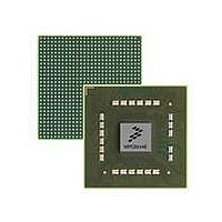
MPC8544VTALF Freescale Semiconductor, MPC8544VTALF Datasheet - Page 30

MPC8544VTALF
Manufacturer Part Number
MPC8544VTALF
Description
MPU POWERQUICC III 783-PBGA
Manufacturer
Freescale Semiconductor
Datasheets
1.MPC8544VTALF.pdf
(117 pages)
2.MPC8544VTALF.pdf
(2 pages)
3.MPC8544VTALF.pdf
(1340 pages)
Specifications of MPC8544VTALF
Processor Type
MPC85xx PowerQUICC III 32-Bit
Speed
667MHz
Voltage
1V
Mounting Type
Surface Mount
Package / Case
783-FCPBGA
Processor Series
MPC85xx
Core
e500
Data Bus Width
32 bit
Maximum Clock Frequency
667 MHz
Maximum Operating Temperature
+ 105 C
Mounting Style
SMD/SMT
Data Ram Size
32 KB
I/o Voltage
1.8 V, 3.3 V
Interface Type
I2C, HSSI, DUART
Minimum Operating Temperature
0 C
Lead Free Status / RoHS Status
Lead free / RoHS Compliant
Features
-
Lead Free Status / Rohs Status
Lead free / RoHS Compliant
Available stocks
Company
Part Number
Manufacturer
Quantity
Price
Company:
Part Number:
MPC8544VTALF
Manufacturer:
Freescale Semiconductor
Quantity:
10 000
Company:
Part Number:
MPC8544VTALFA
Manufacturer:
Freescale Semiconductor
Quantity:
10 000
Enhanced Three-Speed Ethernet (eTSEC), MII Management
Figure 10
8.5
The AC timing specifications for FIFO, GMII, MII, TBI, RGMII, RMII, and RTBI are presented in this
section.
8.5.1
The basis for the AC specifications for the eTSEC FIFO modes is the double data rate RGMII and RTBI
specifications, since they have similar performance and are described in a source-synchronous fashion like
FIFO modes. However, the FIFO interface provides deliberate skew between the transmitted data and
source clock in GMII fashion.
When the eTSEC is configured for FIFO modes, all clocks are supplied from external sources to the
relevant eTSEC interface. That is, the transmit clock must be applied to the eTSECn TSECn_TX_CLK,
while the receive clock must be applied to pin TSECn_RX_CLK. The eTSEC internally uses the transmit
clock to synchronously generate transmit data and outputs an echoed copy of the transmit clock back out
onto the TSECn_GTX_CLK pin (while transmit data appears on TSECn_TXD[7:0], for example). It is
intended that external receivers capture eTSEC transmit data using the clock on TSECn_GTX_CLK as a
source-synchronous timing reference. Typically, the clock edge that launched the data can be used, since
the clock is delayed by the eTSEC to allow acceptable set-up margin at the receiver.
A summary of the FIFO AC specifications appears in
30
At recommended operating conditions with L/TVDD of 3.3 V ± 5% or 2.5 V ± 5%
TX_CLK, GTX_CLK clock period
TX_CLK, GTX_CLK duty cycle
TX_CLK, GTX_CLK peak-to-peak jitter
Rise time TX_CLK (20%–80%)
FIFO, GMII,MII, TBI, RGMII, RMII, and RTBI AC Timing
Specifications
provides the AC test load for SGMII.
FIFO AC Specifications
Parameter/Condition
MPC8544E PowerQUICC III Integrated Processor Hardware Specifications, Rev. 5
Table 28. FIFO Mode Transmit AC Timing Specification
D+ Package
D+ Package
D– Package
Figure 10. SGMII AC Test/Measurement Load
+ Package
Silicon
Pin
Pin
Pin
TX
Symbol
t
t
t
t
FITH
FITR
FITJ
C = C
C = C
FIT
R = 50 Ω
TX
TX
Table 28
Min
45
—
—
—
and
Table
R = 50 Ω
Typ
8.0
50
—
—
29.
Max
0.75
250
55
—
Freescale Semiconductor
Unit
ns
ps
ns
%
Notes
—
—
—
—


