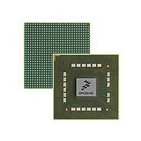
MPC8544VTALF Freescale Semiconductor, MPC8544VTALF Datasheet - Page 61

MPC8544VTALF
Manufacturer Part Number
MPC8544VTALF
Description
MPU POWERQUICC III 783-PBGA
Manufacturer
Freescale Semiconductor
Datasheets
1.MPC8544VTALF.pdf
(117 pages)
2.MPC8544VTALF.pdf
(2 pages)
3.MPC8544VTALF.pdf
(1340 pages)
Specifications of MPC8544VTALF
Processor Type
MPC85xx PowerQUICC III 32-Bit
Speed
667MHz
Voltage
1V
Mounting Type
Surface Mount
Package / Case
783-FCPBGA
Processor Series
MPC85xx
Core
e500
Data Bus Width
32 bit
Maximum Clock Frequency
667 MHz
Maximum Operating Temperature
+ 105 C
Mounting Style
SMD/SMT
Data Ram Size
32 KB
I/o Voltage
1.8 V, 3.3 V
Interface Type
I2C, HSSI, DUART
Minimum Operating Temperature
0 C
Lead Free Status / RoHS Status
Lead free / RoHS Compliant
Features
-
Lead Free Status / Rohs Status
Lead free / RoHS Compliant
Available stocks
Company
Part Number
Manufacturer
Quantity
Price
Company:
Part Number:
MPC8544VTALF
Manufacturer:
Freescale Semiconductor
Quantity:
10 000
Company:
Part Number:
MPC8544VTALFA
Manufacturer:
Freescale Semiconductor
Quantity:
10 000
14.2
Table 54
Figure 40
15 PCI
This section describes the DC and AC electrical specifications for the PCI bus of the MPC8544E.
15.1
Table 55
Freescale Semiconductor
GPIO inputs—minimum pulse width
Note:
1. GPIO inputs and outputs are asynchronous to any visible clock. GPIO outputs should be synchronized before use by any
High-level input voltage
Low-level input voltage
Input current (V
High-level output voltage (OV
Low-level output voltage (OV
Notes:
1. Ranges listed do not meet the full range of the DC specifications of the PCI 2.2 Local Bus Specifications.
2. Note that the symbol V
external synchronous logic. GPIO inputs are required to be valid for at least t
provides the GPIO input and output AC timing specifications.
provides the DC electrical characteristics for the PCI interface.
GPIO AC Electrical Specifications
PCI DC Electrical Characteristics
provides the AC test load for the GPIO.
IN
= 0 V or V
MPC8544E PowerQUICC III Integrated Processor Hardware Specifications, Rev. 5
Parameter
IN
, in this case, represents the OV
Output
IN
DD
DD
= V
Parameter
= min, I
= min, I
DD
Table 54. GPIO Input AC Timing Specifications
Table 55. PCI DC Electrical Characteristics
)
OL
OH
= 2 mA)
= –2mA)
Figure 40. GPIO AC Test Load
Z
0
= 50 Ω
IN
Symbol
symbol referenced in
V
V
V
V
I
IN
OH
OL
IH
IL
R
L
–0.3
Min
2.4
= 50 Ω
—
—
PIWID
2
Symbol
t
PIWID
Table 1
ns to ensure proper operation.
1
OV
OV
and
DD
DD
Max
0.8
0.4
±5
—
Table
/2
Typ
20
+ 0.3
2.
Unit
Unit
μA
ns
V
V
V
V
Notes
Notes
—
—
—
—
1
2
PCI
61


