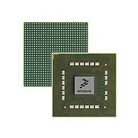
MPC8544VTALF Freescale Semiconductor, MPC8544VTALF Datasheet - Page 107

MPC8544VTALF
Manufacturer Part Number
MPC8544VTALF
Description
MPU POWERQUICC III 783-PBGA
Manufacturer
Freescale Semiconductor
Datasheets
1.MPC8544VTALF.pdf
(117 pages)
2.MPC8544VTALF.pdf
(2 pages)
3.MPC8544VTALF.pdf
(1340 pages)
Specifications of MPC8544VTALF
Processor Type
MPC85xx PowerQUICC III 32-Bit
Speed
667MHz
Voltage
1V
Mounting Type
Surface Mount
Package / Case
783-FCPBGA
Processor Series
MPC85xx
Core
e500
Data Bus Width
32 bit
Maximum Clock Frequency
667 MHz
Maximum Operating Temperature
+ 105 C
Mounting Style
SMD/SMT
Data Ram Size
32 KB
I/o Voltage
1.8 V, 3.3 V
Interface Type
I2C, HSSI, DUART
Minimum Operating Temperature
0 C
Lead Free Status / RoHS Status
Lead free / RoHS Compliant
Features
-
Lead Free Status / Rohs Status
Lead free / RoHS Compliant
Available stocks
Company
Part Number
Manufacturer
Quantity
Price
Company:
Part Number:
MPC8544VTALF
Manufacturer:
Freescale Semiconductor
Quantity:
10 000
Company:
Part Number:
MPC8544VTALFA
Manufacturer:
Freescale Semiconductor
Quantity:
10 000
Note the following:
21.3
Due to large address and data buses, and high operating frequencies, the device can generate transient
power surges and high frequency noise in its power supply, especially while driving large capacitive loads.
This noise must be prevented from reaching other components in the MPC8544E system, and the device
itself requires a clean, tightly regulated source of power. Therefore, it is recommended that the system
designer place at least one decoupling capacitor at each V
of the device. These decoupling capacitors should receive their power from separate V
OV
minimize inductance. Capacitors may be placed directly under the device using a standard escape pattern.
Others may surround the part.
These capacitors should have a value of 0.01 or 0.1 µF. Only ceramic SMT (surface mount technology)
capacitors should be used to minimize lead inductance, preferably 0402 or 0603 sizes.
In addition, it is recommended that there be several bulk storage capacitors distributed around the PCB,
feeding the V
smaller chip capacitors. These bulk capacitors should have a low ESR (equivalent series resistance) rating
to ensure the quick response time necessary. They should also be connected to the power and ground
planes through two vias to minimize inductance. Suggested bulk capacitors—100–330 µF (AVX TPS
tantalum or Sanyo OSCON). However, customers should work directly with their power regulator vendor
for best values and types and quantity of bulk capacitors.
21.4
The SerDes block requires a clean, tightly regulated source of power (SV
jitter on transmit and reliable recovery of data in the receiver. An appropriate decoupling scheme is
outlined below.
Only surface mount technology (SMT) capacitors should be used to minimize inductance. Connections
from all capacitors to power and ground should be done with multiple vias to further reduce inductance.
Freescale Semiconductor
DD
•
•
•
•
•
, GV
AV
Signals on the SerDes interface are fed from the XV
First, the board should have at least 10 × 10-nF SMT ceramic chip capacitors as close as possible
to the supply balls of the device. Where the board has blind vias, these capacitors should be placed
directly below the chip supply and ground connections. Where the board does not have blind vias,
these capacitors should be placed in a ring around the device as close to the supply and ground
connections as possible.
Second, there should be a 1-µF ceramic chip capacitor on each side of the device. This should be
done for all SerDes supplies.
Third, between the device and any SerDes voltage regulator there should be a 10-µF, low
equivalent series resistance (ESR) SMT tantalum chip capacitor and a 100-µF, low ESR SMT
tantalum chip capacitor. This should be done for all SerDes supplies.
Decoupling Recommendations
SerDes Block Power Supply Decoupling Recommendations
DD_
DD
DD
, and LV
SRDS should be a filtered version of SV
, TV
MPC8544E PowerQUICC III Integrated Processor Hardware Specifications, Rev. 5
DD
DD
, BV
; and GND power planes in the PCB, utilizing short low impedance traces to
DD
, OV
DD
, GV
DD
, and LV
DD
DD
DD
.
planes, to enable quick recharging of the
, TV
DD
power plane.
DD
, BV
DD
DD
, OV
and XV
DD
, GV
System Design Information
DD
DD
DD
) to ensure low
, TV
, and LV
DD
, BV
DD
DD
pin
107
,


