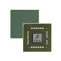
MPC8544VTALF Freescale Semiconductor, MPC8544VTALF Datasheet - Page 10

MPC8544VTALF
Manufacturer Part Number
MPC8544VTALF
Description
MPU POWERQUICC III 783-PBGA
Manufacturer
Freescale Semiconductor
Datasheets
1.MPC8544VTALF.pdf
(117 pages)
2.MPC8544VTALF.pdf
(2 pages)
3.MPC8544VTALF.pdf
(1340 pages)
Specifications of MPC8544VTALF
Processor Type
MPC85xx PowerQUICC III 32-Bit
Speed
667MHz
Voltage
1V
Mounting Type
Surface Mount
Package / Case
783-FCPBGA
Processor Series
MPC85xx
Core
e500
Data Bus Width
32 bit
Maximum Clock Frequency
667 MHz
Maximum Operating Temperature
+ 105 C
Mounting Style
SMD/SMT
Data Ram Size
32 KB
I/o Voltage
1.8 V, 3.3 V
Interface Type
I2C, HSSI, DUART
Minimum Operating Temperature
0 C
Lead Free Status / RoHS Status
Lead free / RoHS Compliant
Features
-
Lead Free Status / Rohs Status
Lead free / RoHS Compliant
Available stocks
Company
Part Number
Manufacturer
Quantity
Price
Company:
Part Number:
MPC8544VTALF
Manufacturer:
Freescale Semiconductor
Quantity:
10 000
Company:
Part Number:
MPC8544VTALFA
Manufacturer:
Freescale Semiconductor
Quantity:
10 000
Electrical Characteristics
10
Three-speed Ethernet I/O voltage
PCI, DUART, PCI Express, system control and power management, I
and JTAG I/O voltage
Local bus I/O voltage
Input voltage
Junction temperature range
Notes:
1. This voltage is the input to the filter discussed in
2. Caution: MV
3. Caution: OV
4. Caution: T/LV
5. Caution: BV
at the AV
power-on reset and power-down sequences.
power-on reset and power-down sequences.
power-on reset and power-down sequences.
power-on reset and power-down sequences.
DD
pin, which may be reduced from V
IN
IN
IN
IN
must not exceed BV
must not exceed OV
must not exceed GV
must not exceed T/ LV
MPC8544E PowerQUICC III Integrated Processor Hardware Specifications, Rev. 5
DDR and DDR2 DRAM signals
DDR and DDR2 DRAM reference
Three-speed Ethernet signals
PCI, Local bus, DUART, SYSCLK, system control
and power management, I
Local bus signals
Characteristic
Table 2. Recommended Operating Conditions (continued)
DD
DD
DD
by more than 0.3 V. This limit may be exceeded for a maximum of 20 ms during
by more than 0.3 V. This limit may be exceeded for a maximum of 20 ms during
DD
by more than 0.3 V. This limit may be exceeded for a maximum of 20 ms during
by more than 0.3 V. This limit may be exceeded for a maximum of 20 ms during
2
C, and JTAG signals
DD
Section 21.2, “PLL Power Supply Filtering,”
by the filter.
2
C,
(eTSEC1)
(eTSEC3)
Symbol
MV
OV
BV
TV
LV
MV
TV
BV
OV
LV
T
REF
DD
DD
DD
DD
IN
j
IN
IN
IN
IN
Recommended
GND to GV
3.3 V ± 165 mV
2.5 V ± 125 mV
3.3 V ± 165 mV
2.5 V ± 125 mV
3.3 V ± 165 mV
3.3 V ± 165 mV
2.5 V ± 125 mV
1.8 V ± 90 mV
GND to GV
GND to BV
GND to OV
GND to TV
GND to LV
0 to 105
and not necessarily the voltage
Value
DD
Freescale Semiconductor
DD
DD
DD
DD
DD
/2
Unit
°C
V
V
V
V
V
V
V
V
Notes
—
4
3
5
2
2
4
5
3


