MPC8347VRADDB Freescale Semiconductor, MPC8347VRADDB Datasheet - Page 95
MPC8347VRADDB
Manufacturer Part Number
MPC8347VRADDB
Description
IC MPU POWERQUICC II 620-PBGA
Manufacturer
Freescale Semiconductor
Series
PowerQUICC II PROr
Specifications of MPC8347VRADDB
Processor Type
MPC83xx PowerQUICC II Pro 32-Bit
Speed
266MHz
Voltage
1.2V
Mounting Type
Surface Mount
Package / Case
620-PBGA
Processor Series
MPC8xxx
Core
e300
Data Bus Width
32 bit
Development Tools By Supplier
MPC8349E-MITXE
Maximum Clock Frequency
266 MHz
Maximum Operating Temperature
+ 105 C
Mounting Style
SMD/SMT
I/o Voltage
1.8 V, 2.5 V, 3.3 V
Minimum Operating Temperature
0 C
Core Size
32 Bit
Program Memory Size
64KB
Cpu Speed
266MHz
Embedded Interface Type
I2C, SPI, USB, UART
Digital Ic Case Style
BGA
No. Of Pins
672
Rohs Compliant
Yes
Lead Free Status / RoHS Status
Lead free / RoHS Compliant
Features
-
Lead Free Status / Rohs Status
Lead free / RoHS Compliant
Available stocks
Company
Part Number
Manufacturer
Quantity
Price
Company:

Part Number:
MPC8347VRADDB
Manufacturer:
Freescale Semiconductor
Quantity:
135
Company:
Part Number:
MPC8347VRADDB
Manufacturer:
Freescale Semiconductor
Quantity:
10 000


22.2
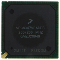
Parts are marked as in the example shown in
23 Document Revision History
Table 72
Freescale Semiconductor
Number
Rev.
11
10
9
provides a revision history of this document.
Part Marking
MPC8347EA PowerQUICC II Pro Integrated Host Processor Hardware Specifications, Rev. 11
11/2010
05/2010
5/2009
Date
Figure 44. Freescale Part Marking for TBGA or PBGA Devices
• In
• In
• In
• Added
• In
• In
• In
• In
for pin LGPL4.
and PBGA from 95.5 Sn/0.5 Cu/4 Ag to 96.5 Sn/3.5 Ag.
and DDR2.
Section 18.3, “Package Parameters for the MPC8347EA
Table
Table
Table
Section 21.7, “Pull-Up Resistor
Table 25
Table
Table
58, updated frequency for DDR2, from 100-200 to 100-133 at core frequency = 533MHz.
70, footnote 1, changed 667(TBGA) to 533(TBGA). footnote 4, added data rate for DDR1
56, added overbar to LCS[4] and LCS[5] signals. In
59, added two columns for the DDR1 and DDR2 memory bus frequency.
Notes
Table 72. Document Revision History
through
ATWLYYWW is the traceability code.
CCCCC is the country code.
MMMMM is the mask number.
YWWLAZ is the assembly traceability code.
8, “EC_GTX_CLK125 AC Timing Specifications.”
:
*MMMMM
Table
MPCnnnnetppaaar
core/platform MHZ
Figure
ATWLYYWW
30, changed V
TBGA/ PBGA
CCCCC
44.
Requirements, updated the list of open drain type pins.
Substantive Change(s)
YWWLAZ
IL
(min) to V
IH
(max) to (20%–80%).
PBGA, changed solder ball for TBGA
Table 55
and
Document Revision History
Table
56, added note
95
Related parts for MPC8347VRADDB
Image
Part Number
Description
Manufacturer
Datasheet
Request
R

Part Number:
Description:
Integrated Host Processor Hardware Specifications
Manufacturer:
FREESCALE [Freescale Semiconductor, Inc]
Datasheet:

Part Number:
Description:
Manufacturer:
Freescale Semiconductor, Inc
Datasheet:
Part Number:
Description:
Manufacturer:
Freescale Semiconductor, Inc
Datasheet:
Part Number:
Description:
Manufacturer:
Freescale Semiconductor, Inc
Datasheet:
Part Number:
Description:
Manufacturer:
Freescale Semiconductor, Inc
Datasheet:
Part Number:
Description:
Manufacturer:
Freescale Semiconductor, Inc
Datasheet:
Part Number:
Description:
Manufacturer:
Freescale Semiconductor, Inc
Datasheet:
Part Number:
Description:
Manufacturer:
Freescale Semiconductor, Inc
Datasheet:
Part Number:
Description:
Manufacturer:
Freescale Semiconductor, Inc
Datasheet:
Part Number:
Description:
Manufacturer:
Freescale Semiconductor, Inc
Datasheet:
Part Number:
Description:
Manufacturer:
Freescale Semiconductor, Inc
Datasheet:
Part Number:
Description:
Manufacturer:
Freescale Semiconductor, Inc
Datasheet:
Part Number:
Description:
Manufacturer:
Freescale Semiconductor, Inc
Datasheet:
Part Number:
Description:
Manufacturer:
Freescale Semiconductor, Inc
Datasheet:
Part Number:
Description:
Manufacturer:
Freescale Semiconductor, Inc
Datasheet: