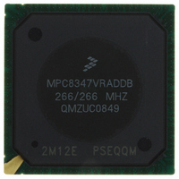
MPC8347VRADDB Freescale Semiconductor, MPC8347VRADDB Datasheet - Page 18

MPC8347VRADDB
Manufacturer Part Number
MPC8347VRADDB
Description
IC MPU POWERQUICC II 620-PBGA
Manufacturer
Freescale Semiconductor
Series
PowerQUICC II PROr
Specifications of MPC8347VRADDB
Processor Type
MPC83xx PowerQUICC II Pro 32-Bit
Speed
266MHz
Voltage
1.2V
Mounting Type
Surface Mount
Package / Case
620-PBGA
Processor Series
MPC8xxx
Core
e300
Data Bus Width
32 bit
Development Tools By Supplier
MPC8349E-MITXE
Maximum Clock Frequency
266 MHz
Maximum Operating Temperature
+ 105 C
Mounting Style
SMD/SMT
I/o Voltage
1.8 V, 2.5 V, 3.3 V
Minimum Operating Temperature
0 C
Core Size
32 Bit
Program Memory Size
64KB
Cpu Speed
266MHz
Embedded Interface Type
I2C, SPI, USB, UART
Digital Ic Case Style
BGA
No. Of Pins
672
Rohs Compliant
Yes
Lead Free Status / RoHS Status
Lead free / RoHS Compliant
Features
-
Lead Free Status / Rohs Status
Lead free / RoHS Compliant
Available stocks
Company
Part Number
Manufacturer
Quantity
Price
Company:
Part Number:
MPC8347VRADDB
Manufacturer:
Freescale Semiconductor
Quantity:
135
Company:
Part Number:
MPC8347VRADDB
Manufacturer:
Freescale Semiconductor
Quantity:
10 000
DDR and DDR2 SDRAM
Table 19
Figure 4
18
At recommended operating conditions with GV
Controller Skew for MDQS—MDQ/MECC/MDM
Notes:
1. t
2. The amount of skew that can be tolerated from MDQS to a corresponding MDQ signal is called t
3. This specification applies only to the DDR interface.
will be captured with MDQS[n]. This should be subtracted from the total timing budget.
determined by the equation: t
value of t
CISKEW
MDQS[n]
MDQ[x]
illustrates the DDR input timing diagram showing the t
provides the input AC timing specifications for the DDR SDRAM interface.
represents the total amount of skew consumed by the controller between MDQS[n] and any corresponding bit that
CISKEW
MCK[n]
MCK[n]
MPC8347EA PowerQUICC II Pro Integrated Host Processor Hardware Specifications, Rev. 11
.
Parameter
Table 19. DDR and DDR2 SDRAM Input AC Timing Specifications
DISKEW
= ± (T/4 – abs (t
DD
Figure 4. DDR Input Timing Diagram
400 MHz
333 MHz
266 MHz
200 MHz
of (1.8 or 2.5 V) ± 5%.
t
t
MCK
DISKEW
CISKEW
Symbol
t
CISKEW
)); where T is the clock period and abs (t
D0
–600
–750
–750
–750
Min
D1
DISKEW
t
DISKEW
timing parameter.
Max
600
750
750
750
DISKEW
Freescale Semiconductor
CISKEW
. This can be
Unit
ps
) is the absolute
Notes
1, 2
—
—
—
3


