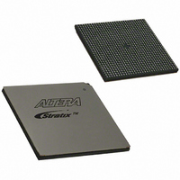
EP1S80B956C7N Altera, EP1S80B956C7N Datasheet - Page 500

EP1S80B956C7N
Manufacturer Part Number
EP1S80B956C7N
Description
IC STRATIX FPGA 80K LE 956-BGA
Manufacturer
Altera
Series
Stratix®r
Datasheet
1.EP1S10F484I6N.pdf
(864 pages)
Specifications of EP1S80B956C7N
Number Of Logic Elements/cells
79040
Number Of Labs/clbs
7904
Total Ram Bits
7427520
Number Of I /o
683
Voltage - Supply
1.425 V ~ 1.575 V
Mounting Type
Surface Mount
Operating Temperature
0°C ~ 85°C
Package / Case
956-BGA
Lead Free Status / RoHS Status
Lead free / RoHS Compliant
Number Of Gates
-
Available stocks
Company
Part Number
Manufacturer
Quantity
Price
- Current page: 500 of 864
- Download datasheet (11Mb)
Receiver Data Realignment
Figure 5–20. Realignment Circuit TXLOADEN Signal Control
Note to
(1)
5–28
Stratix Device Handbook, Volume 2
PLL Output
This figure does not show additional realignment circuitry.
Figure
5–20:
Counter Circuitry
8
SYNC
TXLOADEN signal is generated by the v counter, and when the v counter
is used for realignment, the TXLOADEN signal is generated by the k
counter, as shown in
Realignment Implementation
The realignment signal (SYNC) is used for data realignment and
reframing. An external pin (RX_DATA_ALIGN) or an internal signal
controls the rx_data_align node end. When the rx_data_align
node end is asserted high for at least two low-frequency clock cycles, the
RXLOADEN signal is delayed by one high-frequency clock period and the
parallel bits shift by one bit.
between the high-frequency clock, the RXLOADEN signal, and the parallel
data.
÷ k
÷ v
÷ l
Realignment CLK
Realignment CLK
Realignment
Realignment
Circuit
Circuit
Data
Data
Sync S1
Sync S2
Figure
5–20.
Figure 5–21
Note (1)
Clock
Distribution
Circuitry
shows the timing relationship
CLK1 LVDS
Circuitry
×1 CLK1 to logic array
TXLOADEN
RXLOADEN
×1 CLK2 to logic array
CLK2 LVDS
Circuitry
GCLK/LCLK
Altera Corporation
July 2005
Related parts for EP1S80B956C7N
Image
Part Number
Description
Manufacturer
Datasheet
Request
R

Part Number:
Description:
CYCLONE II STARTER KIT EP2C20N
Manufacturer:
Altera
Datasheet:

Part Number:
Description:
CPLD, EP610 Family, ECMOS Process, 300 Gates, 16 Macro Cells, 16 Reg., 16 User I/Os, 5V Supply, 35 Speed Grade, 24DIP
Manufacturer:
Altera Corporation
Datasheet:

Part Number:
Description:
CPLD, EP610 Family, ECMOS Process, 300 Gates, 16 Macro Cells, 16 Reg., 16 User I/Os, 5V Supply, 15 Speed Grade, 24DIP
Manufacturer:
Altera Corporation
Datasheet:

Part Number:
Description:
Manufacturer:
Altera Corporation
Datasheet:

Part Number:
Description:
CPLD, EP610 Family, ECMOS Process, 300 Gates, 16 Macro Cells, 16 Reg., 16 User I/Os, 5V Supply, 30 Speed Grade, 24DIP
Manufacturer:
Altera Corporation
Datasheet:

Part Number:
Description:
High-performance, low-power erasable programmable logic devices with 8 macrocells, 10ns
Manufacturer:
Altera Corporation
Datasheet:

Part Number:
Description:
High-performance, low-power erasable programmable logic devices with 8 macrocells, 7ns
Manufacturer:
Altera Corporation
Datasheet:

Part Number:
Description:
Classic EPLD
Manufacturer:
Altera Corporation
Datasheet:

Part Number:
Description:
High-performance, low-power erasable programmable logic devices with 8 macrocells, 10ns
Manufacturer:
Altera Corporation
Datasheet:

Part Number:
Description:
Manufacturer:
Altera Corporation
Datasheet:

Part Number:
Description:
Manufacturer:
Altera Corporation
Datasheet:

Part Number:
Description:
Manufacturer:
Altera Corporation
Datasheet:

Part Number:
Description:
CPLD, EP610 Family, ECMOS Process, 300 Gates, 16 Macro Cells, 16 Reg., 16 User I/Os, 5V Supply, 25 Speed Grade, 24DIP
Manufacturer:
Altera Corporation
Datasheet:


