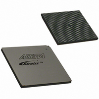
EP1S80B956C7N Altera, EP1S80B956C7N Datasheet - Page 497

EP1S80B956C7N
Manufacturer Part Number
EP1S80B956C7N
Description
IC STRATIX FPGA 80K LE 956-BGA
Manufacturer
Altera
Series
Stratix®r
Datasheet
1.EP1S10F484I6N.pdf
(864 pages)
Specifications of EP1S80B956C7N
Number Of Logic Elements/cells
79040
Number Of Labs/clbs
7904
Total Ram Bits
7427520
Number Of I /o
683
Voltage - Supply
1.425 V ~ 1.575 V
Mounting Type
Surface Mount
Operating Temperature
0°C ~ 85°C
Package / Case
956-BGA
Lead Free Status / RoHS Status
Lead free / RoHS Compliant
Number Of Gates
-
Available stocks
Company
Part Number
Manufacturer
Quantity
Price
- Current page: 497 of 864
- Download datasheet (11Mb)
Receiver Data
Realignment
Altera Corporation
July 2005
Advanced Clear & Enable Control
There are several control signals for clearing and enabling PLLs and their
outputs. You can use these signals to control PLL resynchronization and
to gate PLL output clocks for low-power applications.
The PLLENABLE pin is a dedicated pin that enables and disables Stratix
device enhanced and fast PLLs. When the PLLENABLE pin is low, the
clock output ports are driven by GND and all the PLLs go out of lock.
When the PLLENABLE pin goes high again, the PLLs relock and
resynchronize to the input clocks.
The reset signals are reset/resynchronization inputs for each enhanced
PLL. Stratix devices can drive these input signals from an input pin or
from LEs. When driven high, the PLL counters reset, clearing the PLL
output and placing the PLL out of lock. When driven low again, the PLL
resynchronizes to its input as it relocks.
Most systems using serial differential I/O data transmission require a
certain data-realignment circuit. Stratix devices contain embedded data-
realignment circuitry. While normal I/O operation guarantees that data
is captured, it does not guarantee the parallelization boundary, as this
point is randomly determined based on the power-up of both
communicating devices. The data-realignment circuitry corrects for bit
misalignments by shifting, or delaying, data bits.
Data Realignment Principles of Operation
Stratix devices use a realignment and clock distribution circuitry
(described in
Set the internal rx_data_align node end high to assert the data-
realignment circuitry. When this node is switched from a low to a high
state, the realignment circuitry is activated and the data is delayed by one
bit. To ensure the rising edge of the rx_data_align node end is latched
into the PLL, the rx_data_align node end should stay high for at least
two low-frequency clock cycles.
An external circuit or an internal custom-made state machine using LEs
can generate the signal to pull the rx_data_align node end to a high
state.
When the data realignment circuitry is activated, it generates an internal
pulse Sync S1 or Sync S2 that disables one of the two counters used for the
SERDES operation (described in
counter is disabled for one high-frequency clock cycle, delaying the
“Counter Circuitry” on page
High-Speed Differential I/O Interfaces in Stratix Devices
“Counter Circuitry” on page
Stratix Device Handbook, Volume 2
5–22) for data realignment.
5–22). One
5–25
Related parts for EP1S80B956C7N
Image
Part Number
Description
Manufacturer
Datasheet
Request
R

Part Number:
Description:
CYCLONE II STARTER KIT EP2C20N
Manufacturer:
Altera
Datasheet:

Part Number:
Description:
CPLD, EP610 Family, ECMOS Process, 300 Gates, 16 Macro Cells, 16 Reg., 16 User I/Os, 5V Supply, 35 Speed Grade, 24DIP
Manufacturer:
Altera Corporation
Datasheet:

Part Number:
Description:
CPLD, EP610 Family, ECMOS Process, 300 Gates, 16 Macro Cells, 16 Reg., 16 User I/Os, 5V Supply, 15 Speed Grade, 24DIP
Manufacturer:
Altera Corporation
Datasheet:

Part Number:
Description:
Manufacturer:
Altera Corporation
Datasheet:

Part Number:
Description:
CPLD, EP610 Family, ECMOS Process, 300 Gates, 16 Macro Cells, 16 Reg., 16 User I/Os, 5V Supply, 30 Speed Grade, 24DIP
Manufacturer:
Altera Corporation
Datasheet:

Part Number:
Description:
High-performance, low-power erasable programmable logic devices with 8 macrocells, 10ns
Manufacturer:
Altera Corporation
Datasheet:

Part Number:
Description:
High-performance, low-power erasable programmable logic devices with 8 macrocells, 7ns
Manufacturer:
Altera Corporation
Datasheet:

Part Number:
Description:
Classic EPLD
Manufacturer:
Altera Corporation
Datasheet:

Part Number:
Description:
High-performance, low-power erasable programmable logic devices with 8 macrocells, 10ns
Manufacturer:
Altera Corporation
Datasheet:

Part Number:
Description:
Manufacturer:
Altera Corporation
Datasheet:

Part Number:
Description:
Manufacturer:
Altera Corporation
Datasheet:

Part Number:
Description:
Manufacturer:
Altera Corporation
Datasheet:

Part Number:
Description:
CPLD, EP610 Family, ECMOS Process, 300 Gates, 16 Macro Cells, 16 Reg., 16 User I/Os, 5V Supply, 25 Speed Grade, 24DIP
Manufacturer:
Altera Corporation
Datasheet:


