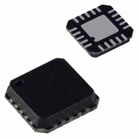
ADF4002BCPZ Analog Devices Inc, ADF4002BCPZ Datasheet - Page 8

ADF4002BCPZ
Manufacturer Part Number
ADF4002BCPZ
Description
IC PLL FREQUENCY SYNTH 20-LFCSP
Manufacturer
Analog Devices Inc
Type
Clock/Frequency Synthesizer (RF), Phase Detectorr
Datasheet
1.ADF4002BCPZ.pdf
(20 pages)
Specifications of ADF4002BCPZ
Design Resources
Very Low Jitter Encode (Sampling) Clocks for High Speed Analog-to-Digital Converters Using ADF4002 (CN0003)
Pll
Yes
Input
CMOS
Output
Clock
Number Of Circuits
1
Ratio - Input:output
2:1
Differential - Input:output
Yes/No
Frequency - Max
400MHz
Divider/multiplier
Yes/No
Voltage - Supply
2.7 V ~ 3.3 V
Operating Temperature
-40°C ~ 85°C
Mounting Type
Surface Mount
Package / Case
20-LFCSP
Frequency-max
400MHz
Pll Type
Frequency Synthesis
Frequency
400MHz
Supply Current
5mA
Supply Voltage Range
2.7V To 3.3V
Digital Ic Case Style
LFCSP
No. Of Pins
20
Operating Temperature Range
-40°C To +85°C
Lead Free Status / RoHS Status
Lead free / RoHS Compliant
For Use With
EVAL-ADF4002EBZ1 - BOARD EVAL FOR ADF4002
Lead Free Status / RoHS Status
Lead free / RoHS Compliant, Lead free / RoHS Compliant
Available stocks
Company
Part Number
Manufacturer
Quantity
Price
Company:
Part Number:
ADF4002BCPZ
Manufacturer:
MICREL
Quantity:
115
Part Number:
ADF4002BCPZ
Manufacturer:
ADI/亚德诺
Quantity:
20 000
Company:
Part Number:
ADF4002BCPZ-RL7
Manufacturer:
ADI
Quantity:
1 497
Part Number:
ADF4002BCPZ-RL7
Manufacturer:
ADI/亚德诺
Quantity:
20 000
ADF4002
THEORY OF OPERATION
REFERENCE INPUT SECTION
The reference input stage is shown in Figure 10. SW1 and SW2
are normally closed switches. SW3 is normally open. When
power-down is initiated, SW3 is closed and SW1 and SW2 are
opened. This ensures that there is no loading of the REF
on power-down.
RF INPUT STAGE
The RF input stage is shown in Figure 11. It is followed by a
2-stage limiting amplifier to generate the CML clock levels
needed for the N counter.
N COUNTER
The N CMOS counter allows a wide ranging division ratio in
the PLL feedback counter. Division ratios from 1 to 8191 are
allowed.
N and R Relationship
The N counter makes it possible to generate output frequencies
that are spaced only by the reference frequency divided by R.
RF
RF
REF
IN
IN
A
B
IN
NC
POWER-DOWN
GENERATOR
SW1
CONTROL
Figure 10. Reference Input Stage
BIAS
Figure 11. RF Input Stage
NO
NC
SW2
500Ω
SW3
100kΩ
1.6V
500Ω
BUFFER
AGND
AV
DD
TO R COUNTER
IN
pin
Rev. A | Page 8 of 20
The equation for the VCO frequency is
where:
f
oscillator (VCO).
N is the preset divide ratio of binary 13-bit counter (1 to 8191).
f
R COUNTER
The 14-bit R counter allows the input reference frequency to be
divided down to produce the reference clock to the phase
frequency detector (PFD). Division ratios from 1 to 16,383 are
allowed.
PHASE FREQUENCY DETECTOR (PFD) AND
CHARGE PUMP
The PFD takes inputs from the R counter and N counter and
produces an output proportional to the phase and frequency
difference between them. Figure 13 is a simplified schematic.
The PFD includes a programmable delay element that controls
the width of the antibacklash pulse. This pulse ensures that
there is no dead zone in the PFD transfer function, and
minimizes phase noise and reference spurs. Two bits in the
reference counter latch (ABP2 and ABP1) control the width of
the pulse. See Figure 16 for details. The smallest antibacklash
pulse width is not recommended.
VCO
REFIN
R DIVIDER
N DIVIDER
is the output frequency of external voltage controlled
is the external reference frequency oscillator.
f
VCO
Figure 13. PFD Simplified Schematic and Timing (In Lock)
HI
HI
=
N
D2
INPUT STAGE
D1
CLR1
CLR2
×
FROM RF
U2
U1
f
Q1
Q2
REFIN
R
PROGRAMMABLE
UP
DOWN
ABP2
Figure 12. N Counter
COUNTER LATCH
DELAY
COUNTER
13-BIT N
FROM N
ABP1
U3
TO PFD
CPGND
V
P
CHARGE
PUMP
CP


