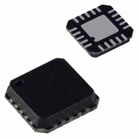
ADF4002BCPZ Analog Devices Inc, ADF4002BCPZ Datasheet - Page 17

ADF4002BCPZ
Manufacturer Part Number
ADF4002BCPZ
Description
IC PLL FREQUENCY SYNTH 20-LFCSP
Manufacturer
Analog Devices Inc
Type
Clock/Frequency Synthesizer (RF), Phase Detectorr
Datasheet
1.ADF4002BCPZ.pdf
(20 pages)
Specifications of ADF4002BCPZ
Design Resources
Very Low Jitter Encode (Sampling) Clocks for High Speed Analog-to-Digital Converters Using ADF4002 (CN0003)
Pll
Yes
Input
CMOS
Output
Clock
Number Of Circuits
1
Ratio - Input:output
2:1
Differential - Input:output
Yes/No
Frequency - Max
400MHz
Divider/multiplier
Yes/No
Voltage - Supply
2.7 V ~ 3.3 V
Operating Temperature
-40°C ~ 85°C
Mounting Type
Surface Mount
Package / Case
20-LFCSP
Frequency-max
400MHz
Pll Type
Frequency Synthesis
Frequency
400MHz
Supply Current
5mA
Supply Voltage Range
2.7V To 3.3V
Digital Ic Case Style
LFCSP
No. Of Pins
20
Operating Temperature Range
-40°C To +85°C
Lead Free Status / RoHS Status
Lead free / RoHS Compliant
For Use With
EVAL-ADF4002EBZ1 - BOARD EVAL FOR ADF4002
Lead Free Status / RoHS Status
Lead free / RoHS Compliant, Lead free / RoHS Compliant
Available stocks
Company
Part Number
Manufacturer
Quantity
Price
Company:
Part Number:
ADF4002BCPZ
Manufacturer:
MICREL
Quantity:
115
Part Number:
ADF4002BCPZ
Manufacturer:
ADI/亚德诺
Quantity:
20 000
Company:
Part Number:
ADF4002BCPZ-RL7
Manufacturer:
ADI
Quantity:
1 497
Part Number:
ADF4002BCPZ-RL7
Manufacturer:
ADI/亚德诺
Quantity:
20 000
APPLICATIONS
VERY LOW JITTER ENCODE CLOCK FOR HIGH
SPEED CONVERTERS
Figure 20 shows the ADF4002 with a VCXO to provide the
encode clock for a high speed analog-to-digital converter (ADC).
The converter used in this application is an AD9215-80, a 12-bit
converter that accepts up to an 80 MHz encode clock. To realize
a stable low jitter clock, use a 77.76 MHz, narrow band VCXO.
This example assumes a 19.44 MHz reference clock.
To minimize the phase noise contribution of the ADF4002, the
smallest multiplication factor of 4 is used. Thus, the R divider is
programmed to 1, and the N divider is programmed to 4.
The charge pump output of the ADF4002 (Pin 2) drives the
loop filter. The loop filter bandwidth is optimized for the best
possible rms jitter, a key factor in the signal-to-noise ratio
(SNR) of the ADC. Too narrow a bandwidth allows the VCXO
noise to dominate at small offsets from the carrier frequency.
Too wide a bandwidth allows the ADF4002 noise to dominate at
offsets where the VCXO noise is lower than the ADF4002 noise.
Thus, the intersection of the VCXO noise and the ADF4002 in-
band noise is chosen as the optimum loop filter bandwidth.
The design of the loop filter uses the ADIsimPLL (Version 3.0)
and is available as a free download from www.analog.com/pll.
The rms jitter is measured at <1.2 ps. This level is lower than
the maximum allowable 6 ps rms required to ensure the
theoretical SNR performance of 59 dB for this converter.
The setup shown in Figure 20 using the ADF4002, AD9215, and
HSC-ADC-EVALA-SC allows the user to quickly and effectively
determine the suitability of the converter and encode clock. The
SPI® interface is used to control the ADF4002, and the USB inter-
face helps control the operation of the AD9215-80. The controller
board sends back FFT information to the PC that, if using an
ADC analyzer, provides all conversion results from the ADC.
19.44MHz
500kHz, 1.8V p-p
TCXO:
AGILENT:
R = 1
N = 4
ADF4002
PD
Figure 20. ADF4002 as Encode Clock
A
VCXO: 77.76MHz
IN
SPI
AD9215-80
ENCODE
CLOCK
HC-ADC-EVALA-SC
PC
Rev. A | Page 17 of 20
PFD
As the ADF4002 permits both R and N counters to be pro-
grammed to 1, the part can effectively be used as a standalone
PFD and charge pump. This is particularly useful in either a
clock cleaning application or a high performance LO. Addi-
tionally, the very low normalized phase noise floor (−222 dBc/Hz)
enables very low in-band phase noise levels. It is possible to
operate the PFD up to a maximum frequency of 104 MHz.
In Figure 21, the reference frequency equals the PFD; therefore,
R = 1. The charge pump output integrates into a stable control
voltage for the VCXO, and the output from the VCXO is divided
down to the desired PFD frequency using an external divider.
INTERFACING
The ADF4002 has a simple SPI-compatible serial interface for
writing to the device. CLK, DATA, and LE control the data
transfer. When the latch enable (Pin LE) goes high, the 24 bits
that have been clocked into the input register on each rising
edge of CLK are transferred to the appropriate latch. For more
information, see Figure 2 for the timing diagram and Table 6 for
the latch truth table.
The maximum allowable serial clock rate is 20 MHz. This
means that the maximum update rate possible for the device is
833 kHz, or one update every 1.2 μs. This is certainly more than
adequate for systems that have typical lock times in hundreds of
microseconds.
REF
IN
8
V
7
REF
DD
3
ADF4002
15
IN
4
9
16
RF
RF
V
R
P
SET
IN
IN
Figure 21. ADF4002 as a PFD
A
B
2
6
5
1
100pF
10kΩ
100pF
DECOUPLING CAPACITORS AND
INTERFACE SIGNALS HAVE BEEN
OMITTED FROM THE DIAGRAM IN
THE INTERESTS OF GREATER
CLARITY.
FILTER
LOOP
51Ω
EXTERNAL PRESCALER
GND
V
V
CC
CC
V
CC
GND
VCXO
VCO
OR
100pF
ADF4002
100pF
18Ω
18Ω
18Ω
RF
OUT


