FDS6982AS Fairchild Semiconductor, FDS6982AS Datasheet
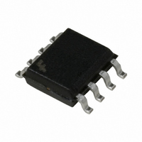
MOSFET N-CH DUAL 30V SO-8

FDS6982AS

Manufacturer Part Number
FDS6982AS
Description
MOSFET N-CH DUAL 30V SO-8
Manufacturer
Fairchild Semiconductor
Series
PowerTrench®r
Datasheet

Specifications of FDS6982AS

Fet Type
2 N-Channel (Dual)
Fet Feature
Logic Level Gate
Rds On (max) @ Id, Vgs
28 mOhm @ 6.3A, 10V
Drain To Source Voltage (vdss)
30V
Current - Continuous Drain (id) @ 25° C
6.3A, 8.6A
Vgs(th) (max) @ Id
3V @ 250µA
Gate Charge (qg) @ Vgs
15nC @ 10V
Input Capacitance (ciss) @ Vds
610pF @ 10V
Power - Max
900mW
Mounting Type
Surface Mount
Package / Case
8-SOIC (3.9mm Width)
Configuration
Dual Dual Drain
Transistor Polarity
N-Channel
Resistance Drain-source Rds (on)
0.028 Ohm @ 10 V Ohm @ Q1
Forward Transconductance Gfs (max / Min)
32 S, 19 S
Drain-source Breakdown Voltage
30 V
Gate-source Breakdown Voltage
+ /- 20 V
Continuous Drain Current
6.3 A @ Q1
Power Dissipation
2000 mW
Maximum Operating Temperature
+ 150 C
Mounting Style
SMD/SMT
Minimum Operating Temperature
- 55 C
Lead Free Status / RoHS Status
Lead free / RoHS Compliant
Other names
FDS6982AS
FDS6982ASTR

Available stocks

Company
Part Number
Manufacturer
Quantity
Price
Part Number:
FDS6982AS
Manufacturer:
FSC
Quantity:
30 000
Part Number:
FDS6982AS
Manufacturer:
FSC
Quantity:
12 500
Part Number:
FDS6982AS
Manufacturer:
FAIRCHILD
Quantity:
50 000
Part Number:
FDS6982AS
Manufacturer:
ON/安森美
Quantity:
20 000
Company:
Part Number:
FDS6982AS
Quantity:
56
Company:
Part Number:
FDS6982AS
Quantity:
20 000
Company:
Part Number:
FDS6982AS
Quantity:
4 500
Part Number:
FDS6982AS-NL
Manufacturer:
FAI-Pb free
Quantity:
55
Part Number:
FDS6982AS/ROHS
Manufacturer:
FAIRCHILD/仙童
Quantity:
20 000
FDS6982AS
Dual Notebook Power Supply N-Channel PowerTrench
General Description
The FDS6982AS is designed to replace two single SO-
8
DC:DC power supplies that provide various peripheral
voltages for notebook computers and other battery
powered electronic devices. FDS6982AS contains two
unique 30V, N-channel, logic level, PowerTrench
MOSFETs designed to maximize power conversion
efficiency. The high-side switch (Q1) is designed with
specific emphasis on reducing switching losses while
the low-side switch (Q2) is optimized to reduce
conduction losses.
Schottky diode using Fairchild’s monolithic SyncFET
technology.
Applications
• Notebook
©2008 Fairchild Semiconductor Corporation
Absolute Maximum Ratings
V
V
I
P
T
Thermal Characteristics
R
R
Package Marking and Ordering Information
Symbol
D
J
DSS
GSS
D
θJA
θJC
, T
Device Marking
MOSFETs and Schottky diode in synchronous
FDS6982AS
STG
D2
SO-8
Drain-Source Voltage
Gate-Source Voltage
Drain Current
Power Dissipation for Dual Operation
Power Dissipation for Single Operation
Operating and Storage Junction Temperature Range
Thermal Resistance, Junction-to-Ambient
Thermal Resistance, Junction-to-Case
D2
Q2 also includes an integrated
D1
D1
- Continuous
- Pulsed
S2
FDS6982AS
Device
G2
Parameter
S1
G1
T
A
= 25°C unless otherwise noted
Reel Size
13”
(Note 1a)
(Note 1a)
(Note 1b)
(Note 1c)
(Note 1a)
(Note 1)
Features
Low gate charge (21nC typical)
Q2:
Q1:
6.3A, 30V
Low gate charge (11nC typical)
8.6A, 30V
Optimized to minimize conduction losses
Includes SyncFET Schottky body diode
Optimized for low switching losses
5
6
7
8
Q2
±20
8.6
30
30
Tape width
R
R
R
R
12mm
–55 to +150
Q1
Q2
DS(on)
DS(on)
DS(on)
DS(on)
®
1.6
0.9
78
40
SyncFET
2
1
max= 13.5mΩ @ V
max= 16.5mΩ @ V
max= 28.0mΩ @ V
max= 35.0mΩ @ V
Q1
±20
6.3
30
20
4
3
2
1
May 2008
2500 units
FDS6982AS Rev B1
Quantity
GS
GS
GS
GS
Units
°C/W
°C/W
= 10V
= 4.5V
= 10V
= 4.5V
°C
W
V
V
A
tmM

Related parts for FDS6982AS

FDS6982AS Summary of contents

Page 1

... FDS6982AS Dual Notebook Power Supply N-Channel PowerTrench General Description The FDS6982AS is designed to replace two single SO- 8 MOSFETs and Schottky diode in synchronous DC:DC power supplies that provide various peripheral voltages for notebook computers and other battery powered electronic devices. FDS6982AS contains two ...

Page 2

... 6 6 125° 1.0 MHz V = 15mV 1.0 MHz 10V Ω GS GEN 4.5V Ω GS GEN mV/° 500 µ ±100 1 1 –3.1 mV/°C Q1 –4 13.5 mΩ 16 20 1250 pF Q1 610 Q2 410 pF Q1 180 Q2 130 1.4 Ω FDS6982AS Rev B1 ...

Page 3

... A (Note (Note 1.3 A (Note determined by the user's board design. θCA b) 125°C/W when mounted 0.02 in pad copper Type Min Typ Max Units 3 1 2 0.5 Q2 0.7 V 0.6 1.0 Q2 0.8 1 135°C/W when mounted on a minimum pad. FDS6982AS Rev B1 ...

Page 4

... Figure 6. Body Diode Forward Voltage Variation with Source Current and Temperature. = 2.5V 3.0V 3.5V 4.0V 4.5V 6.0V 10V DRAIN CURRENT ( 4 125 GATE TO SOURCE VOLTAGE (V) GS Gate-to-Source Voltage 125 -55 C 0.2 0.4 0 BODY DIODE FORWARD VOLTAGE (V) SD FDS6982AS Rev 0.8 ...

Page 5

... Figure 10. Single Pulse Maximum 0.01 0 TIME (sec 1MHz iss C oss DRAIN TO SOURCE VOLTAGE (V) DS SINGLE PULSE R = 135°C/W θ 25° 100 1000 t , TIME (sec) 1 Power Dissipation. R ( θJA θ 135°C/W θJA P(pk ( θJA Duty Cycle 100 1000 FDS6982AS Rev B1 30 ...

Page 6

... Figure 17. Body Diode Forward Voltage Variation with Source Current and Temperature. = 3.0V GS 3.5V 4.0V 4.5V 6.0V 10V DRAIN CURRENT ( 3. 125 GATE TO SOURCE VOLTAGE ( Gate-to-Source Voltage 125 -55 C 0.2 0.4 0.6 0 BODY DIODE FORWARD VOLTAGE (V) SD FDS6982AS Rev 1.4 ...

Page 7

... Figure 21. Single Pulse Maximum 0.01 0 TIME (sec 1MHz iss C oss DRAIN TO SOURCE VOLTAGE (V) DS SINGLE PULSE R = 135°C/W θ 25° 100 1000 t , TIME (sec) 1 Power Dissipation. R ( θJA θ 135°C/W θJA P(pk ( θJA Duty Cycle 100 1000 FDS6982AS Rev B1 ...

Page 8

... Schottky diode in parallel with a MOSFET. Figure 23 shows the reverse recovery characteristic of the FDS6982AS. Time: 10nS/DIV Figure 23. FDS6982AS SyncFET body diode reverse recovery characteristic. For comparison purposes, Figure 24 shows the reverse recovery characteristics of the body diode of an equivalent size MOSFET produced without SyncFET (FDS6982) ...

Page 9

... Pulse Width ≤ 1µs Duty Cycle ≤ 0.1% Figure 30. Switching Time Test Circuit + Figure 27. Unclamped Inductive Waveforms + 10V DUT Charge, (nC) Figure 29. Gate Charge Waveform d(ON 90% + DUT 50% 10% 0V Figure 31. Switching Time Waveforms BV DSS G(TOT OFF t d(OFF 90% 10% 10% 90% 50% Pulse Width FDS6982AS Rev B1 ...

Page 10

... Fairchild Semiconductor. The datasheet is for reference information only. ® The Power Franchise tm TinyBoost™ TinyBuck™ ® TinyLogic TINYOPTO™ TinyPower™ TinyPWM™ TinyWire™ µSerDes™ ® UHC Ultra FRFET™ UniFET™ VCX™ VisualMax™ Definition Rev. I34 FDS6982AS Rev.B1 ...

Related keywords