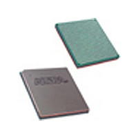
EP1S30F1020C5N Altera, EP1S30F1020C5N Datasheet - Page 87

EP1S30F1020C5N
Manufacturer Part Number
EP1S30F1020C5N
Description
Stratix
Manufacturer
Altera
Datasheet
1.EP1S30F1020C5N.pdf
(276 pages)
Specifications of EP1S30F1020C5N
Family Name
Stratix
Number Of Logic Blocks/elements
32470
# I/os (max)
726
Frequency (max)
500MHz
Process Technology
0.13um (CMOS)
Operating Supply Voltage (typ)
1.5V
Logic Cells
32470
Ram Bits
3317184
Operating Supply Voltage (min)
1.425V
Operating Supply Voltage (max)
1.575V
Operating Temp Range
0C to 85C
Operating Temperature Classification
Commercial
Mounting
Surface Mount
Pin Count
1020
Package Type
FC-FBGA
Lead Free Status / Rohs Status
Compliant
Available stocks
Company
Part Number
Manufacturer
Quantity
Price
Company:
Part Number:
EP1S30F1020C5N
Manufacturer:
ALTERA
Quantity:
455
Part Number:
EP1S30F1020C5N
Manufacturer:
ALTERA/阿尔特拉
Quantity:
20 000
- Current page: 87 of 276
- Download datasheet (4Mb)
PLLs & Clock
Networks
Altera Corporation
July 2005
clock signals are routed from LAB row clocks and are generated from
specific LAB rows at the DSP block interface. The LAB row source for
control signals, data inputs, and outputs is shown in
Stratix devices provide a hierarchical clock structure and multiple PLLs
with advanced features. The large number of clocking resources in
combination with the clock synthesis precision provided by enhanced
and fast PLLs provides a complete clock management solution.
Global & Hierarchical Clocking
Stratix devices provide 16 dedicated global clock networks, 16 regional
clock networks (four per device quadrant), and 8 dedicated fast regional
clock networks (for EP1S10, EP1S20, and EP1S25 devices), and
16 dedicated fast regional clock networks (for EP1S30 EP1S40, and
EP1S60, and EP1S80 devices). These clocks are organized into a
hierarchical clock structure that allows for up to 22 clocks per device
region with low skew and delay. This hierarchical clocking scheme
provides up to 48 unique clock domains within Stratix devices.
1
2
3
4
5
6
7
8
Table 2–17. DSP Block Signal Sources & Destinations
LAB Row at
Interface
signa
aclr0
accum_sload0
addnsub1
clock0
ena0
aclr1
clock1
ena1
aclr2
clock2
ena2
sign_b
clock3
ena3
clear3
accum_sload1
addnsub3
Control Signals
Generated
A1[17..0]
B1[17..0]
A2[17..0]
B2[17..0]
A3[17..0]
B3[17..0]
A4[17..0]
B4[17..0]
Stratix Device Handbook, Volume 1
Data Inputs
Table
Stratix Architecture
OA[17..0]
OB[17..0]
OC[17..0]
OD[17..0]
OE[17..0]
OF[17..0]
OG[17..0]
OH[17..0]
Data Outputs
2–17.
2–73
Related parts for EP1S30F1020C5N
Image
Part Number
Description
Manufacturer
Datasheet
Request
R

Part Number:
Description:
CYCLONE II STARTER KIT EP2C20N
Manufacturer:
Altera
Datasheet:

Part Number:
Description:
CPLD, EP610 Family, ECMOS Process, 300 Gates, 16 Macro Cells, 16 Reg., 16 User I/Os, 5V Supply, 35 Speed Grade, 24DIP
Manufacturer:
Altera Corporation
Datasheet:

Part Number:
Description:
CPLD, EP610 Family, ECMOS Process, 300 Gates, 16 Macro Cells, 16 Reg., 16 User I/Os, 5V Supply, 15 Speed Grade, 24DIP
Manufacturer:
Altera Corporation
Datasheet:

Part Number:
Description:
Manufacturer:
Altera Corporation
Datasheet:

Part Number:
Description:
CPLD, EP610 Family, ECMOS Process, 300 Gates, 16 Macro Cells, 16 Reg., 16 User I/Os, 5V Supply, 30 Speed Grade, 24DIP
Manufacturer:
Altera Corporation
Datasheet:

Part Number:
Description:
High-performance, low-power erasable programmable logic devices with 8 macrocells, 10ns
Manufacturer:
Altera Corporation
Datasheet:

Part Number:
Description:
High-performance, low-power erasable programmable logic devices with 8 macrocells, 7ns
Manufacturer:
Altera Corporation
Datasheet:

Part Number:
Description:
Classic EPLD
Manufacturer:
Altera Corporation
Datasheet:

Part Number:
Description:
High-performance, low-power erasable programmable logic devices with 8 macrocells, 10ns
Manufacturer:
Altera Corporation
Datasheet:

Part Number:
Description:
Manufacturer:
Altera Corporation
Datasheet:

Part Number:
Description:
Manufacturer:
Altera Corporation
Datasheet:

Part Number:
Description:
Manufacturer:
Altera Corporation
Datasheet:

Part Number:
Description:
CPLD, EP610 Family, ECMOS Process, 300 Gates, 16 Macro Cells, 16 Reg., 16 User I/Os, 5V Supply, 25 Speed Grade, 24DIP
Manufacturer:
Altera Corporation
Datasheet:


