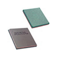
EP1S30F1020C5N Altera, EP1S30F1020C5N Datasheet - Page 131

EP1S30F1020C5N
Manufacturer Part Number
EP1S30F1020C5N
Description
Stratix
Manufacturer
Altera
Datasheet
1.EP1S30F1020C5N.pdf
(276 pages)
Specifications of EP1S30F1020C5N
Family Name
Stratix
Number Of Logic Blocks/elements
32470
# I/os (max)
726
Frequency (max)
500MHz
Process Technology
0.13um (CMOS)
Operating Supply Voltage (typ)
1.5V
Logic Cells
32470
Ram Bits
3317184
Operating Supply Voltage (min)
1.425V
Operating Supply Voltage (max)
1.575V
Operating Temp Range
0C to 85C
Operating Temperature Classification
Commercial
Mounting
Surface Mount
Pin Count
1020
Package Type
FC-FBGA
Lead Free Status / Rohs Status
Compliant
Available stocks
Company
Part Number
Manufacturer
Quantity
Price
Company:
Part Number:
EP1S30F1020C5N
Manufacturer:
ALTERA
Quantity:
455
Part Number:
EP1S30F1020C5N
Manufacturer:
ALTERA/阿尔特拉
Quantity:
20 000
- Current page: 131 of 276
- Download datasheet (4Mb)
Altera Corporation
July 2005
Notes to
(1)
(2)
(3)
(4)
(5)
DDR SDRAM (1),
DDR SDRAM - side banks (2),
QDR SRAM
QDRII SRAM
ZBT SRAM
EP1S10
EP1S20
Table 2–26. External RAM Support in EP1S60 & EP1S80 Devices
Table 2–27. DQS & DQ Bus Mode Support
Device
These maximum clock rates apply if the Stratix device uses DQS phase-shift circuitry to interface with DDR
SDRAM. DQS phase-shift circuitry is only available in the top and bottom I/O banks (I/O banks 3, 4, 7, and 8).
For more information on DDR SDRAM, see AN 342: Interfacing DDR SDRAM with Stratix & Stratix GX Devices.
DDR SDRAM is supported on the Stratix device side I/O banks (I/O banks 1, 2, 5, and 6) without dedicated DQS
phase-shift circuitry. The read DQS signal is ignored in this mode. Numbers are preliminary.
For more information on QDR or QDRII SRAM, see AN 349: QDR SRAM Controller Reference Design for Stratix &
Stratix GX Devices.
For more information on ZBT SRAM, see AN 329: ZBT SRAM Controller Reference Design for Stratix & Stratix GX
Devices.
DDR Memory Type
Table
(5)
(4)
(4)
2–26:
672-pin BGA
672-pin FineLine BGA
484-pin FineLine BGA
780-pin FineLine BGA
484-pin FineLine BGA
672-pin BGA
672-pin FineLine BGA
780-pin FineLine BGA
(2)
Package
In addition to six I/O registers and one input latch in the IOE for
interfacing to these high-speed memory interfaces, Stratix devices also
have dedicated circuitry for interfacing with DDR SDRAM. In every
Stratix device, the I/O banks at the top (I/O banks 3 and 4) and bottom
(I/O banks 7 and 8) of the device support DDR SDRAM up to 200 MHz.
These pins support DQS signals with DQ bus modes of ×8, ×16, or ×32.
Table 2–27
per device.
(3)
SSTL-2
SSTL-2
1.5-V HSTL
1.5-V HSTL
LVTTL
I/O Standard
shows the number of DQ and DQS buses that are supported
(Part 1 of 2)
Number of ×8
Groups
12
16
18(4)
16(3)
-5 Speed Grade
20
(2)
(3)
Note (1)
167
150
133
167
200
Maximum Clock Rate (MHz)
Number of ×16
Groups
Stratix Device Handbook, Volume 1
7
7
7
-6 Speed Grade -7 Speed Grade
0
0
(5)
(5)
(5)
167
133
133
167
200
Number of ×32
Stratix Architecture
Groups
0
4
4
4
4
133
133
133
133
167
2–117
Related parts for EP1S30F1020C5N
Image
Part Number
Description
Manufacturer
Datasheet
Request
R

Part Number:
Description:
CYCLONE II STARTER KIT EP2C20N
Manufacturer:
Altera
Datasheet:

Part Number:
Description:
CPLD, EP610 Family, ECMOS Process, 300 Gates, 16 Macro Cells, 16 Reg., 16 User I/Os, 5V Supply, 35 Speed Grade, 24DIP
Manufacturer:
Altera Corporation
Datasheet:

Part Number:
Description:
CPLD, EP610 Family, ECMOS Process, 300 Gates, 16 Macro Cells, 16 Reg., 16 User I/Os, 5V Supply, 15 Speed Grade, 24DIP
Manufacturer:
Altera Corporation
Datasheet:

Part Number:
Description:
Manufacturer:
Altera Corporation
Datasheet:

Part Number:
Description:
CPLD, EP610 Family, ECMOS Process, 300 Gates, 16 Macro Cells, 16 Reg., 16 User I/Os, 5V Supply, 30 Speed Grade, 24DIP
Manufacturer:
Altera Corporation
Datasheet:

Part Number:
Description:
High-performance, low-power erasable programmable logic devices with 8 macrocells, 10ns
Manufacturer:
Altera Corporation
Datasheet:

Part Number:
Description:
High-performance, low-power erasable programmable logic devices with 8 macrocells, 7ns
Manufacturer:
Altera Corporation
Datasheet:

Part Number:
Description:
Classic EPLD
Manufacturer:
Altera Corporation
Datasheet:

Part Number:
Description:
High-performance, low-power erasable programmable logic devices with 8 macrocells, 10ns
Manufacturer:
Altera Corporation
Datasheet:

Part Number:
Description:
Manufacturer:
Altera Corporation
Datasheet:

Part Number:
Description:
Manufacturer:
Altera Corporation
Datasheet:

Part Number:
Description:
Manufacturer:
Altera Corporation
Datasheet:

Part Number:
Description:
CPLD, EP610 Family, ECMOS Process, 300 Gates, 16 Macro Cells, 16 Reg., 16 User I/Os, 5V Supply, 25 Speed Grade, 24DIP
Manufacturer:
Altera Corporation
Datasheet:


