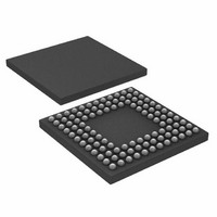
ADUC7121BBCZ-RL Analog Devices Inc, ADUC7121BBCZ-RL Datasheet - Page 50

ADUC7121BBCZ-RL
Manufacturer Part Number
ADUC7121BBCZ-RL
Description
PRECISION ANALOG MCU I.C
Manufacturer
Analog Devices Inc
Series
MicroConverter® ADuC7xxxr
Datasheet
1.ADUC7121BBCZ.pdf
(96 pages)
Specifications of ADUC7121BBCZ-RL
Core Processor
ARM7
Core Size
16/32-Bit
Speed
41.78MHz
Connectivity
I²C, SPI, UART/USART
Peripherals
POR, PWM, WDT
Number Of I /o
32
Program Memory Size
126KB (63K x 16)
Program Memory Type
FLASH
Ram Size
8K x 8
Voltage - Supply (vcc/vdd)
3 V ~ 3.6 V
Data Converters
A/D 9x12b, D/A 4x12b
Oscillator Type
Internal
Operating Temperature
-10°C ~ 95°C
Package / Case
108-LFBGA, CSPBGA
Lead Free Status / RoHS Status
Lead free / RoHS Compliant
Eeprom Size
-
Lead Free Status / RoHS Status
Lead free / RoHS Compliant
Other names
ADUC7121BBCZ-RL
ADUC7121BBCZ-RLTR
ADUC7121BBCZ-RLTR
Available stocks
Company
Part Number
Manufacturer
Quantity
Price
Company:
Part Number:
ADUC7121BBCZ-RL
Manufacturer:
Analog Devices Inc
Quantity:
10 000
ADuC7121
DIGITAL PERIPHERALS
PWM GENERAL OVERVIEW
The ADuC7121 integrates a 6-channel PWM interface. The PWM
outputs can be configured to drive an H-bridge or can be used as
standard PWM outputs. On power-up, the PWM outputs default
to H-bridge mode. This ensures that the motor is turned off by
default. In standard PWM mode, the outputs are arranged as three
pairs of PWM pins. Users have control over the period of each
pair of outputs and over the duty cycle of each individual output.
In all modes, the PWMxCOMx MMRs control the point at
which the PWM outputs change state. An example of the first pair
of PWM outputs (PWM1 and PWM2) is shown in Figure 33.
Table 68. PWM MMRs
Name
PWMCON1
PWM1COM1
PWM1COM2
PWM1COM3
PWM1LEN
PWM2COM1
PWM2COM2
PWM2COM3
PWM2LEN
PWM3COM1
PWM3COM2
PWM3COM3
PWM3LEN
PWMCON2
PWMICLR
HIGH SIDE
LOW SIDE
(PWM1)
(PWM2)
PWM1COM3
PWM1COM2
PWM1COM1
PWM1LEN
Figure 33. PWM Timing
Function
PWM control
Compare Register 1 for PWM Output 1 and PWM Output 2
Compare Register 2 for PWM Output 1 and PWM Output 2
Compare Register 3 for PWM Output 1 and PWM Output 2
Frequency control for PWM Output 1 and PWM Output 2
Compare Register 1 for PWM Output 3 and PWM Output 4
Compare Register 2 for PWM Output 3 and PWM Output 4
Compare Register 3 for PWM Output 3 and PWM Output 4
Frequency control for PWM Output 3 and PWM Output 4
Compare Register 1 for PWM Output 5 and PWM Output 6
Compare Register 2 for PWM Output 5 and PWM Output 6
Compare Register 3 for PWM Output 5 and PWM Output 6
Frequency control for PWM Output 5 and PWM Output 6
PWM convert start control
PWM interrupt clear
Rev. 0 | Page 50 of 96
The PWM clock is selectable via PWMCON1 with one of the
following values: UCLK divide-by-2, 4, 8, 16, 32, 64, 128, or
256. The length of a PWM period is defined by PWMxLEN.
The PWM waveforms are set by the count value of the 16-bit
timer and the compare registers contents as shown with the
PWM1 and PWM2 waveforms above.
The low-side waveform, PWM2, goes high when the timer
count reaches PWM1LEN, and it goes low when the timer
count reaches the value held in PWM1COM3 or when the
high-side waveform PWM1 goes low.
The high-side waveform, PWM1, goes high when the timer
count reaches the value held in PWM1COM1, and it goes low
when the timer count reaches the value held in PWM1COM2.


