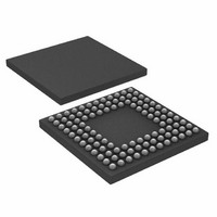
ADUC7121BBCZ-RL Analog Devices Inc, ADUC7121BBCZ-RL Datasheet - Page 55

ADUC7121BBCZ-RL
Manufacturer Part Number
ADUC7121BBCZ-RL
Description
PRECISION ANALOG MCU I.C
Manufacturer
Analog Devices Inc
Series
MicroConverter® ADuC7xxxr
Datasheet
1.ADUC7121BBCZ.pdf
(96 pages)
Specifications of ADUC7121BBCZ-RL
Core Processor
ARM7
Core Size
16/32-Bit
Speed
41.78MHz
Connectivity
I²C, SPI, UART/USART
Peripherals
POR, PWM, WDT
Number Of I /o
32
Program Memory Size
126KB (63K x 16)
Program Memory Type
FLASH
Ram Size
8K x 8
Voltage - Supply (vcc/vdd)
3 V ~ 3.6 V
Data Converters
A/D 9x12b, D/A 4x12b
Oscillator Type
Internal
Operating Temperature
-10°C ~ 95°C
Package / Case
108-LFBGA, CSPBGA
Lead Free Status / RoHS Status
Lead free / RoHS Compliant
Eeprom Size
-
Lead Free Status / RoHS Status
Lead free / RoHS Compliant
Other names
ADUC7121BBCZ-RL
ADUC7121BBCZ-RLTR
ADUC7121BBCZ-RLTR
Available stocks
Company
Part Number
Manufacturer
Quantity
Price
Company:
Part Number:
ADUC7121BBCZ-RL
Manufacturer:
Analog Devices Inc
Quantity:
10 000
Table 74. GPxCON MMR Bit Designations
Bit
31:30
29:28
27:26
25:24
23:22
21:20
19:18
17:16
15:14
13:12
11:10
9:8
7:6
5:4
3:2
1:0
GPxPAR Registers
The GPxPAR registers program the parameters for Port 0, Port 1,
Port 2, and Port 3. Note that the GPxDAT MMR must always be
written after changing the GPxPAR MMR.
Name:
Address:
Default value:
Access:
Name:
Address:
Default value:
Access:
Name:
Address:
Default value:
Access:
Name:
Address:
Default value:
Access:
Description
Reserved
Select function of the Px.7 pin
Reserved
Select function of the Px.6 pin
Reserved
Select function of the Px.5 pin
Reserved
Select function of the Px.4 pin
Reserved
Select function of the Px.3 pin
Reserved
Select function of the Px.2 pin
Reserved
Select function of the Px.1 pin
Reserved
Select function of the Px.0 pin
GP0PAR
0xFFFF0D2C
0x20000000
Read and write
GP1PAR
0xFFFF0D3C
0x00000000
Read and write
GP2PAR
0xFFFF0D4C
0x00000000
Read and write
GP3PAR
0xFFFF0D5C
0x00222222
Read and write
Rev. 0 | Page 55 of 96
Table 75. GPxPAR MMR Bit Designations
Bit
31:29
28
27:25
24
23:21
20
19:17
16
15:13
12
11:9
8
7:5
4
3:1
0
GPxDAT Register
GPxDAT is a Port x configuration and data register. It configures
the direction of the GPIO pins of Port x, sets the output value
for the pins configured as output, and receives and stores the
input value of the pins configured as inputs.
Name:
Address:
Default value:
Access:
Name:
Address:
Default value:
Access:
Name:
Address:
Default value:
Access:
Description
Reserved
Pull-up disable Px.7 pin
Set to 1 to enable the pull-up
Clear to 0 to disable the pull-up
Reserved
Pull-up disable Px.6 pin
Reserved
Pull-up disable Px.5 pin
Reserved
Pull-up disable Px.4 pin
Reserved
Pull-up disable Px.3 pin
Reserved
Pull-up disable Px.2 pin
Reserved
Pull-up disable Px.1 pin
Reserved
Pull-up disable Px.0 pin
GP0DAT
0xFFFF0D20
0x000000XX
Read and write
GP1DAT
0xFFFF0D30
0x000000XX
Read and write
GP2DAT
0xFFFF0D40
0x000000XX
Read and write
ADuC7121


