ADUC7121BBCZ-RL Analog Devices Inc, ADUC7121BBCZ-RL Datasheet
ADUC7121BBCZ-RL
Specifications of ADUC7121BBCZ-RL
ADUC7121BBCZ-RLTR
Available stocks


Related parts for ADUC7121BBCZ-RL


ADUC7121BBCZ-RL Summary of contents
Page 1
FEATURES Analog input/output 9-channel, 12-bit, 1 MSPS ADC 2 differential pairs with input PGA 7 general-purpose inputs (differential or single-ended) Fully differential and single-ended modes analog input range REF 5 low noise current digital-to-analog converters (IDACs) ...
Page 2
ADuC7121 TABLE OF CONTENTS Features .............................................................................................. 1 Applications....................................................................................... 1 Functional Block Diagram .............................................................. 1 Revision History ............................................................................... 3 General Description ......................................................................... 4 Specifications..................................................................................... 5 Timing Specifications ................................................................ 10 Absolute Maximum Ratings.......................................................... 15 ESD Caution................................................................................ 15 Pin Configuration and Function Descriptions........................... ...
Page 3
REVISION HISTORY 1/11—Revision 0: Initial Version Rev Page ADuC7121 ...
Page 4
ADuC7121 GENERAL DESCRIPTION The ADuC7121 is a fully integrated, 1 MSPS, 12-bit data acquisi- tion system incorporating a high performance multichannel ADC, 16-bit/32-bit MCU, and Flash®/EE memory on a single chip. The ADC consists seven single-ended inputs ...
Page 5
SPECIFICATIONS AV = IOV = 3 3 2.0 V ± 5 otherwise noted. Table 1. Parameter ADC CHANNEL SPECIFICATIONS ADC Power-Up Time Accuracy Resolution Integral Nonlinearity Differential Nonlinearity ...
Page 6
ADuC7121 Parameter PADC1 INPUT Full-Scale Input Range 4 Input Leakage at PADC1x Resolution 4 Gain Error 4 Gain Drift 4 Offset 4 Offset Drift PADC1x-Compliant Range ON-CHIP VOLTAGE REFERENCE Output Voltage 7 Accuracy 4 Reference Temperature Coefficient Power Supply Rejection ...
Page 7
Parameter LINE REGULATION IDAC4 IDAC3 IDAC2 IDAC1 IDAC0 LOAD REGULATION IDAC4 IDAC3 IDAC2 IDAC1 IDAC0 4 ACPSRR PULL-DOWN NMOS 4 Speed Voltage DAC (VDAC) CHANNEL 9 DC Accuracy Resolution Relative Accuracy Differential Nonlinearity Calculated Offset Error Actual Offset Error 10 ...
Page 8
ADuC7121 Parameter 11 TEMPERATURE SENSOR Voltage Output at 25°C Voltage Temperature Coefficient Accuracy POWER SUPPLY MONITOR (PSM) IOV Trip Point Selection DD Power Supply Trip Point Accuracy POWER-ON RESET WATCHDOG TIMER (WDT) Timeout Period FLASH/EE MEMORY Endurance 12 13 Data ...
Page 9
Parameter Digital Power Supply Current IOV Current in Normal Mode DD IOV Current in Pause Mode IOV Current in Sleep Mode DD Additional Power Supply Currents ADC IDAC DAC ESD TESTS HBM Passed Up to FICDM Passed ...
Page 10
ADuC7121 TIMING SPECIFICATIONS 2 Table Timing in Fast Mode (400 kHz) Parameter Description t SCL low pulse width L t SCL high pulse width H t Start condition hold time SHD t Data setup time DSU t ...
Page 11
Table 4 SPI Master Mode Timing (Phase Mode = 1) Parameter Description t SPICLK low pulse width SL t SPICLK high pulse width SH t Data output valid after SPICLK edge DAV t Data input setup time before SPICLK edge ...
Page 12
ADuC7121 Table 5. SPI Master Mode Timing (Phase Mode = 0) Parameter Description t SPICLK low pulse width SL t SPICLK high pulse width SH t Data output valid after SPICLK edge DAV t Data output setup before SPICLK edge ...
Page 13
Table 6. SPI Slave Mode Timing (Phase Mode = 1) Parameter Description CS to the SPICLK edge SPICLK low pulse width SL t SPICLK high pulse width SH t Data output valid after SPICLK edge DAV t ...
Page 14
ADuC7121 Table 7. SPI Slave Mode Timing (Phase Mode = 0) Parameter Description SPICLK edge CS t SPICLK low pulse width SL t SPICLK high pulse width SH t Data output valid after SPICLK edge DAV ...
Page 15
ABSOLUTE MAXIMUM RATINGS AGND = 25°C, unless otherwise noted. A Table 8. Parameter AV to IOV DD DD AGND to DGND IOV to IOGND AGND DD DD Digital Input Voltage to IOGND Digital Output ...
Page 16
ADuC7121 PIN CONFIGURATION AND FUNCTION DESCRIPTIONS Table 9. Pin Function Descriptions Pin No. Mnemonic C12 RST D11 P0.0/SCL0/PLAI[5] E11 P0.1/SDA0/PLAI[4] C3 P0.2/SPICLK/ADC /PLAO[13] BUSY D3 P0.3/MISO/PLAO[12]/SYNC E3 P0.4/MOSI/PLAI[11]/TRIP F3 P0.5/CS/PLAI[10]/ADC CONVST G3 P0.6/MRST/PLAI[2] G10 P0.7/TRST/PLAI[ ...
Page 17
Pin No. Mnemonic C2 P1.0/SIN/SCL1/PLAI[7] D2 P1.1/SOUT/SDA1/PLAI[6] C10 P1.2/TDI/PLAO[15] D10 P1.3/TDO/PLAO[14] H3 P1.4/PWM1/ECLK/XCLK/PLAI[8] J3 P1.5/PWM2/PLAI[9] B3 P1.6/PLAO[5] B2 P1.7/PLAO[4] F11 P2.0/IRQ0/PLAI[13] G11 P2.1/IRQ1/PLAI[12] H11 P2.2/PLAI[1] J11 P2.3/IRQ2/PLAI[14] H10 P2.4/PWM5/PLAO[7] J10 P2.5/PWM6/PLAO[6] C1 P2.6/IRQ3/PLAI[15] C9 P2.7/PLAI[0] C4 P3.0/PLAO[0] C11 P3.1/PLAO[1] 1 ...
Page 18
ADuC7121 Pin No. Mnemonic D1 P3.2/IRQ4/PWM3/PLAO[2] E1 P3.3/IRQ5/PWM4/PLAO[3] E2 P3.4/PLAO[8] F2 P3.5/PLAO[9] D12 P3.6/PLAO[10] E12 P3.7/BM/PLAO[11 _2.5 REF L5 V _1.2 REF B8 I REF K6 BUF_VREF1 K7 BUF_VREF2 L6 PADC0P M5 PADC0N L7 PADC1P M8 PADC1N K5 ...
Page 19
Pin No. Mnemonic A6 C _IDAC4 DAMP A8 IDAC3 A7 PVDD_IDAC3 C8 C _IDAC3 DAMP A5 IDAC2 C5 PVDD_IDAC2 B4 C _IDAC2 DAMP A4 IDAC1 A1 IDAC1 A3 PVDD_IDAC1 A2 PVDD_IDAC1 B1 C _IDAC1 DAMP A12 IDAC0 A9 IDAC0 A11 ...
Page 20
ADuC7121 TERMINOLOGY ADC SPECIFICATIONS Integral Nonlinearity Integral nonlinearity (INL) is the maximum deviation of any code from a straight line passing through the endpoints of the ADC transfer function. The endpoints of the transfer function are zero scale, a point ...
Page 21
OVERVIEW OF THE ARM7TDMI CORE The ARM7™ core is a 32-bit reduced instruction set computer (RISC). It uses a single 32-bit bus for instruction and data. The length of the data can be 8 bits, 16 bits bits. ...
Page 22
ADuC7121 ARM REGISTERS ARM7TDMI has a total of 37 registers: 31 general-purpose registers and 6 status registers. Each operating mode has dedicated banked registers. When writing user level programs, 15 general-purpose 32-bit registers (R0 to R14), the program counter (R15), ...
Page 23
MEMORY ORGANIZATION The ADuC7121 incorporates three separate blocks of memory SRAM and two on-chip Flash/EE memory. There are 126 kB of on-chip Flash/EE memory available to the user, and the remaining 2 kB are ...
Page 24
ADuC7121 0xFFFF0746 IDAC 0xFFFF0700 0xFFFF05DF DAC 0xFFFF0580 0xFFFF0524 ADC 0xFFFF0500 0xFFFFFFFF 0xFFFF04A8 0xFFFF0FBC BANDGAP REFERENCE 0xFFFF0480 0xFFFF0F80 0xFFFF0448 0xFFFF0EA8 POWER SUPPLY MONITOR 0xFFFF0440 0xFFFF0E80 0xFFFF0418 0xFFFF0E28 PLL AND OSCILLATOR CONTROL 0xFFFF0400 0xFFFF0E00 0xFFFF0394 0xFFFF0D78 GENERAL PURPOSE TIMER 4 0xFFFF0D00 0xFFFF0380 ...
Page 25
Table 13. PLL Base Address = 0xFFFF0400 Address Name Byte Access Type 0x0404 POWKEY1 2 W 0x0408 POWCON 1 R/W 0x040C POWKEY2 2 W 0x0410 PLLKEY1 2 W 0x0414 PLLCON 1 R/W 0x0418 PLLKEY2 2 W Table 14. PSM Base ...
Page 26
ADuC7121 Address Name Byte Access Type 0x0924 I2C1DIV 2 R/W 0x0928 I2C1SCTL 2 R/W 0x092C I2C1SSTA 2 R 0x0930 I2C1SRX 1 R 0x0934 I2C1STX 1 W 0x0938 I2C1ALT 1 R/W 0x093C I2C1ID0 1 R/W 0x0940 I2C1ID1 1 R/W 0x0944 I2C1ID2 ...
Page 27
ADC CIRCUIT OVERVIEW The analog-to-digital converter (ADC) incorporates a fast, multichannel, 12-bit ADC. It can operate from a 3 3.6 V supply and is capable of providing a throughput MSPS when the clock source ...
Page 28
ADuC7121 Fully Differential Mode The amplitude of the differential signal is the difference between the signals applied to the V and V IN+ IN− Therefore, the maximum amplitude of the differential IN− signal is − p-p ...
Page 29
The input level for PGA is limited to a maximum value of AVDD − 1.2 V and minimum value of 0 ensure that the amplifiers are not saturated. The input buffer is a rail-to-rail buffer. It can accept ...
Page 30
ADuC7121 Table 29. ADCCON MMR Bit Designations (Address = 0xFFFF0500, Default Value = 0x00000A00) Bit Value Description 31:16 These bits are reserved. 15 Positive ADC buffer bypass. 0 Set the user to enable the positive ADC buffer. ...
Page 31
Table 30. ADCCP MMR Bit Designations Bit Value Description 7:5 Reserved 4:0 Positive channel selection bits 00000 PADC0P 00001 PADC1P 00010 Reserved 00011 Reserved 00100 Reserved 00101 Reserved 00110 ADC4 00111 ADC5 01000 ADC6 01001 ADC7 01010 ADC8 01011 ...
Page 32
ADuC7121 CHANNEL+ AIN0 A SW1 MUX SW3 C SW2 S CHANNEL– A AIN11 B V REF Figure 18. ADC Acquisition Phase When the ADC starts a conversion (see Figure 19), SW3 opens, and SW1 and SW2 move ...
Page 33
ADuC7121 ADC0 V REF ADC1 Figure 24. Buffering Differential Inputs When no amplifier is used to drive the analog input, limit the source impedance to values lower than 1 kΩ. The maximum source impedance depends on the amount of total ...
Page 34
ADuC7121 POWER SUPPLY MONITOR The power supply monitor on the ADuC7121 indicates when the IOVDD supply pin drops below one of two supply trip points. The monitor function is controlled via the PSMCON register. If enabled in the IRQEN or ...
Page 35
NONVOLATILE FLASH/EE MEMORY FLASH/EE MEMORY OVERVIEW The ADuC7121 incorporates Flash/EE memory technology on chip to provide the user with nonvolatile, in circuit reprogram- mable memory space. Similar to EEPROM, flash memory can be programmed in system at a byte level, ...
Page 36
ADuC7121 writing to the Flash/EE memory; each bit protects four pages, that is, 2 kB. Write protection is activated for all access types. FEE1PRO and FEE1HID similarly protect the second 64 kB block. All 32 bits of this are used ...
Page 37
Table 41. FEE0PRO and FEE0HID MMR Bit Designations Bit Description 31 Read protection. Cleared by the user to protect Block 0. Set by the user to allow reading Block 0. 30:0 Write protection for Page 123 to Page 120, for ...
Page 38
ADuC7121 Bit Description 1 Command fail. Set automatically when a command completes unsuccessfully. Cleared automatically when reading FEExSTA register. 0 Command complete. Set by MicroConverter when a command is complete. Cleared automatically when reading FEExSTA register. FEE0MOD Register Name: FEE0MOD ...
Page 39
EXECUTION TIME FROM SRAM AND FLASH/EE This section describes SRAM and Flash/EE access times during execution for applications where execution time is critical. Execution from SRAM Fetching instructions from SRAM takes one clock cycle because the access time of the ...
Page 40
ADuC7121 Reset Operation There are four types of reset: external reset, power-on reset, watchdog expiration, and software force. The RSTSTA register indicates the source of the last reset and RSTCLR clears the RSTSTA register. These registers can be used during ...
Page 41
OTHER ANALOG PERIPHERALS DIGITAL-TO-ANALOG CONVERTERS The ADuC7121 incorporates four buffered 12-bit voltage output string digital-to-analog converters (DACs) on chip. Each DAC has a rail-to-rail voltage output buffer capable of driving 5 kΩ/100 pF. Each DAC has three selectable ranges: 0 ...
Page 42
ADuC7121 Table 49 DACxCON Registers (Default Value = 0x100, Read/Write Access) Name DAC0CON DAC1CON DAC2CON DAC3CON Table 50. DAC0CON MMR Bit Designations Bit Value Name Description 15:9 0 Reserved DACPD DAC power-down. Set by the user to set ...
Page 43
Using the DACs The on-chip DAC architecture consists of a resistor string DAC followed by an output buffer amplifier. The functional equivalent is shown in Figure 29 REF EXT_REF Figure 29. DAC ...
Page 44
ADuC7121 The reference current of each IDAC is generated by a precision internal band gap voltage reference and an external precision resistor, and as such, the gain error of each IDAC is impacted by the accuracy of the external resistor. ...
Page 45
VOLTAGE REFERENCE IDAC MMRs Table 53. IDAC Control Registers (Read and Write Access) Name Address (Hex) IDAC0CON 0xFFFF0700 IDAC1CON 0xFFFF070C IDAC2CON 0xFFFF0718 IDAC3CON 0xFFFF0724 IDAC4CON 0xFFFF0730 TDSCON 0xFFFF073C IDAC0PULLDOWN 0xFFFF0744 Table 54. IDACxCON MMR Bit Designations Bit Name Value Description ...
Page 46
ADuC7121 Table 56. IDAC0PULLDOWN MMR Bit Designations Bit Value Name Description 7:6 Reserved These bits are set the user Pulldown IDAC0 pull-down. Set the user to pull down the IDAC0 pin as ...
Page 47
The operating mode, clocking mode, and programmable clock divider are controlled via two MMRs, PLLCON (see Table 65) and POWCON (see Table 66). PLLCON controls the operating mode of the clock system, and POWCON controls the core clock frequency and ...
Page 48
ADuC7121 Table 63. Operating Modes Mode Core Peripherals Active On On Pause On Nap Sleep Stop Table 64. Typical Current Consumption at 25°C PC[2:0] Mode 000 Active 33.1 001 Pause 22.7 010 Nap 3.8 011 Sleep 0.4 ...
Page 49
MMRs and Keys To prevent accidental programming, a certain sequence must be followed when writing in the PLLCON and POWCON registers (see Table 67). PLLKEYx Registers Name: PLLKEY1 Address: 0xFFFF0410 Default value: 0x0000 Access: Write only Name: PLLKEY2 Address: 0xFFFF0418 ...
Page 50
ADuC7121 DIGITAL PERIPHERALS PWM GENERAL OVERVIEW The ADuC7121 integrates a 6-channel PWM interface. The PWM outputs can be configured to drive an H-bridge or can be used as standard PWM outputs. On power-up, the PWM outputs default to H-bridge mode. ...
Page 51
Table 69. PWMCON1 MMR Bit Designations (Address = 0xFFFF0F80, Default Value = 0x0012) Bit Name Description 15 Reserved This bit is reserved. 14 SYNC Enables PWM synchronization. Set the user so that all PWM counters are reset ...
Page 52
ADuC7121 In H-bridge mode, HMODE = 1 and Table 69 determine the PWM outputs, as listed in Table 70. Table 70. PWM Output Selection PWMCOM1 MMR PWM Outputs ENA HOFF POINV DIR PWM1 PWM2 ...
Page 53
GENERAL-PURPOSE INPUT/OUTPUT The ADuC7121 provides 32 general-purpose, bidirectional input/output (GPIO) pins. All I/O pins are 5 V tolerant, meaning that the GPIOs support an input voltage general, many of the GPIO pins have multiple functions (see ...
Page 54
ADuC7121 Table 73. GPIO Pin Function Designations Port Pin 00 0 P0.0 GPIO P0.1 GPIO P0.2 GPIO P0.3 GPIO P0.4 GPIO P0.5 GPIO P0.6 GPIO P0.7 GPIO 1 P1.0 GPIO P1.1 GPIO 1 P1.2 TDI (JTAG) 1 P1.3 TDO (JTAG) ...
Page 55
Table 74. GPxCON MMR Bit Designations Bit Description 31:30 Reserved 29:28 Select function of the Px.7 pin 27:26 Reserved 25:24 Select function of the Px.6 pin 23:22 Reserved 21:20 Select function of the Px.5 pin 19:18 Reserved 17:16 Select function ...
Page 56
ADuC7121 Name: GP3DAT Address: 0xFFFF0D50 Default value: 0x000000XX Access: Read and write Table 76. GPxDAT MMR Bit Designations Bit Description 31:24 Direction of the data. Set the user to configure the GPIO pin as an output. Cleared ...
Page 57
Table 79. GPxOCE MMR Bit Designations Bit Description 31:8 Reserved. 7 GPIO Px.7 open collector enable. Set the user to enable the open collector. Set the user to disable the open collector. 6 GPIO ...
Page 58
ADuC7121 UART SERIAL INTERFACE The ADuC7121 features a 16,450-compatible UART. The UART is a full-duplex, universal, asynchronous receiver/transmitter. A UART performs serial-to-parallel conversion on data characters received from a peripheral device, and parallel-to-serial conver- sion on data characters received from ...
Page 59
UART TX Register Write to this 8-bit register to transmit data using the UART. Name: COMTX Address: 0xFFFF0800 Access: Write only UART RX Register This 8-bit register is read from to receive data transmitted using the UART. Name: COMRX Address: ...
Page 60
ADuC7121 Table 81. COMCON0 MMR Bit Designations Bit Name 7 DLAB 6 BRK EPS 3 PEN 2 STOP WLS UART Control Register 1 This 8-bit register controls the operation of the UART in conjunction ...
Page 61
UART Status Register 0 Name: COMSTA0 Address: 0xFFFF0814 Default value: 0x60 Access: Read only Function: This 8-bit read-only register reflects the current status on the UART. Table 83. COMSTA0 MMR Bit Designations Bit Name 7 6 TEMT 5 THRE 4 ...
Page 62
ADuC7121 UART Interrupt Enable Register 0 This 8-bit register enables and disables the individual UART interrupt sources. Name: COMIEN0 Address: 0xFFFF0804 Default value: 0x00 Access: Read and write Table 84. COMIEN0 MMR Bit Designations Bit Name Description ...
Page 63
I C PERIPHERALS 2 The ADuC7121 incorporates two I C peripherals that may be 2 configured as a fully I C-compatible bus master device fully I C-compatible bus slave device. Both peripherals are identical. The ...
Page 64
ADuC7121 • I2CxADR0[0] is the read/ write bit REGISTERS 2 The I C peripheral interfaces consists of a number of MMRs. These are described in the following section Master Registers Master ...
Page 65
I C Master Status Register 2 This 16-bit MMR status register in master mode. Name: I2C0MSTA, I2C1MSTA Address: 0xFFFF0884, 0xFFFF0904 Default value: 0x0000, 0x0000 Access: Read only Table 88 I2CxMSTA MMR Bit Designations Bit Name Description ...
Page 66
ADuC7121 Master Receive Registers 2 This 8-bit MMR is the I C master receive register. Name: I2C0MRX, I2C1MRX Address: 0xFFFF0888, 0xFFFF0908 Default value: 0x00 Access: Read only Master Transmit Registers 2 This 8-bit MMR ...
Page 67
I C Master Clock Control Register This MMR controls the frequency of the I the master on to the SCL pin. Name: I2C0DIV, I2C1DIV Address: 0xFFFF08A4, 0xFFFF0924 Default value: 0x1F1F Access: Read and write Table 93. I2CxDIV MMR Bit ...
Page 68
ADuC7121 Table 94. I2CxSCTL MMR Bit Designations Bit Name Description 15:11 Reserved bits. 10 I2CSTXENI Slave transmit interrupt enable bit. Set this bit to enable an interrupt after a slave transmits a byte. Clear this interrupt source. 9 I2CSRXENI Slave ...
Page 69
I C Slave Status Registers 2 These 16-bit MMRs are the I C status registers in slave mode. Name: I2C0SSTA, I2C1SSTA Address: 0xFFFF08AC, 0xFFFF092C Default value: 0x0000, 0x0000 Access: Read and write Table 95. I2CxSSTA MMR Bit Designations Bit ...
Page 70
ADuC7121 Bit Name Description 4 I2CSRxFO Slave Rx FIFO overflow. This bit is set to 1 when a byte is written to the Rx FIFO when it is already full. This bit is cleared in all other conditions ...
Page 71
I C Slave Receive Registers 2 This 8-bit MMR is the I C slave receive register. Name: I2C0SRX, I2C1SRX Address: 0xFFFF08B0, 0xFFFF0930 Default value: 0x00 Access: Read only Slave Transmit Registers 2 This 8-bit MMR is ...
Page 72
ADuC7121 COMMON REGISTERS FIFO Status Registers These 16-bit MMRs contain the status of the Rx/Tx FIFOs in both master and slave modes. Name: I2C0FSTA Address: 0xFFFF08CC Default value: 0x0000 Access: Read and write Name: ...
Page 73
SERIAL PERIPHERAL INTERFACE The ADuC7121 integrates a complete hardware serial peri- pheral interface (SPI) on-chip. SPI is an industry standard, synchronous serial interface that allows eight bits of data to be synchronously transmitted and simultaneously received, that is, full duplex ...
Page 74
ADuC7121 Table 97. SPISTA MMR Bit Designations Bit Name Description 15:12 Reserved bits. 11 SPIREX SPI Rx FIFO excess bytes present. This bit is set when there are more bytes in the Rx FIFO than indicated in the SPIMDE bits ...
Page 75
Table 98. SPICON MMR Bit Designations Bit Name Description 15:14 SPIMDE SPI IRQ mode bits. These bits configure when the Tx/Rx interrupts occur in a transfer. [00 interrupt occurs when one byte has been transferred. Rx interrupt occurs ...
Page 76
ADuC7121 PROGRAMMABLE LOGIC ARRAY (PLA) The ADuC7121 integrates a fully programmable logic array (PLA) that consists of two independent but interconnected PLA blocks. Each block consists of eight PLA elements, giving each part a total of 16 PLA elements. Each ...
Page 77
PLA MMRS INTERFACE The PLA peripheral interface consists of the 21 MMRs described in the following sections. PLAELMx Registers PLAELMx are Element 0 to Element 15 control registers. They configure the input and output mux of each element, select the ...
Page 78
ADuC7121 PLACLK Register PLACLK is the clock selection for the flip-flops of Block 0 and Block 1. The maximum frequency when using the GPIO pins as the clock input for the PLA blocks is 41.78 MHz. Name: PLACLK Address: 0xFFFF0B40 ...
Page 79
PLADOUT Register PLADOUT is a data output MMR for PLA. This register is always updated. Name: PLADOUT Address: 0xFFFF0B50 Default value: 0x00000000 Access: Read only Table 107. PLADOUT MMR Bit Descriptions Bit Description 31:16 Reserved. 15:0 Output bit from Element ...
Page 80
ADuC7121 INTERRUPT SYSTEM Table 108. IRQ/FIQ MMRs Bit Designations Bit Description 0 All interrupts OR’ed (FIQ only) 1 Software interrupt 2 Timer0 3 Timer1 4 Timer2 or wake-up timer 5 Timer3 or watchdog timer 6 Timer4 7 IDAC fault 8 ...
Page 81
Name: IRQSIG Address: 0xFFFF0004 Default value: 0x00000000 Access: Read only IRQEN Register IRQEN provides the value of the current enable mask. When a bit is set to 1, the corresponding source request is enabled to create an IRQ exception. When ...
Page 82
ADuC7121 FIQCLR FIQCLR is a write-only register that allows the FIQEN register to clear to mask an interrupt source. Each bit that is set to 1 clears the corresponding bit in the FIQEN register without affecting the remaining bits. The ...
Page 83
VIC MMRs IRQBASE Register The vector base register, IRQBASE, is used to point to the start address of memory used to store 32 pointer addresses. These pointer addresses are the addresses of the individual interrupt service routines. Name: IRQBASE Address: ...
Page 84
ADuC7121 IRQP2 Register Name: IRQP2 Address: 0xFFFF0028 Default value: 0x00000000 Access: Read and write Table 114. IRQP2 MMR Bit Designations Bit Name Description 31 Reserved Reserved bit. 30:28 PWMPI A priority level can be set for ...
Page 85
FIQVEC Register The FIQ interrupt vector register, FIQVEC points to a memory address containing a pointer to the interrupt service routine of the currently active FIQ. Read this register only when an FIQ occurs and FIQ interrupt nesting has been ...
Page 86
ADuC7121 Bit Value Name 5:4 11 IRQ2SRC[1: 3:2 11 IRQ1SRC[1: 1:0 11 IRQ0SRC[1: IRQCLRE Register Name: IRQCLRE Address: 0xFFFF0038 Default value: 0x00000000 Access: Read and write Description External IRQ2 triggers on ...
Page 87
TIMERS The ADuC7121 has five general purpose timers/counters. • Timer0 • Timer1 • Timer2 or wake-up timer • Timer3 or watchdog timer • Timer4 The five timers in their normal mode of operation can be either free-running or periodic. In ...
Page 88
ADuC7121 Timer0 Capture Register This is a 16-bit register that holds the 16-bit value captured by an enabled IRQ event; available in 16-bit mode only. Name: T0CAP Address: 0xFFFF0314 Default value: 0x0000 Access: Read only Timer0 Control Register This 17-bit ...
Page 89
Table 124. Timer1 Interface Registers Register Description T1LD 32-bit register. Holds 32-bit unsigned integers. This register is read only. T1VAL 32-bit register. Holds 32-bit unsigned integers. T1CAP 32-bit register; Holds 32-bit unsigned integers. This register is read only. T1CLRI 8-bit ...
Page 90
ADuC7121 TIMER2—WAKE-UP TIMER Timer2 is a 32-bit wake-up timer, count down or count up, with a programmable prescaler. The prescaler is clocked directly from one of four clock sources, namely, the core clock (default selection), the internal 32.768 kHz oscillator, ...
Page 91
TIMER3—WATCHDOG TIMER 16-BIT LOAD 16-BIT LOW POWER PRESCALER UP/DOWN 32.768kHz 1, 16, OR 256 COUNTER TIMER3 VALUE Figure 38. Timer3 Block Diagram Timer3 has two modes of operation: normal mode and watchdog mode. The watchdog timer is used to recover ...
Page 92
ADuC7121 Table 129. T3CON MMR Bit Designations Bit Value Description 16:9 These bits are reserved and should be written user code. 8 Count up/down enable. Set by user code to configure Timer3 to count up. Cleared by ...
Page 93
TIMER4—GENERAL-PURPOSE TIMER Timer4 is a 32-bit general-purpose timer, count down or count up, with a programmable prescaler. The prescaler source can be the 32 kHz oscillator, the core clock, or PLL undivided output. This source can be scaled by a ...
Page 94
ADuC7121 Table 130. T4CON MMR Bit Designations Bit Value Description 31:18 Reserved. Set by the user Event select bit. Set by the user to enable time capture of an event. Cleared by the user to disable time ...
Page 95
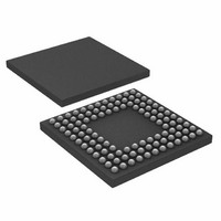
... OUTLINE DIMENSIONS BALL A1 PAD CORNER * 1.40 MAX ORDERING GUIDE 1 Model Temperature Range ADuC7121BBCZ −10°C to +95°C ADuC7121BBCZ-RL −10°C to +95°C EVAL-ADuC7121QSPZ RoHS Compliant Part. 7.10 7. 5.50 BSC SQ 0.50 BSC TOP VIEW DETAIL A DETAIL A 0.15 MIN 0.35 0.30 ...
Page 96
ADuC7121 NOTES refers to a communications protocol originally developed by Philips Semiconductors (now NXP Semiconductors). ©2011 Analog Devices, Inc. All rights reserved. Trademarks and registered trademarks are the property of their respective owners. D09492-0-1/11(0) Rev ...