ADUC7121BBCZ-RL Analog Devices Inc, ADUC7121BBCZ-RL Datasheet - Page 5
ADUC7121BBCZ-RL
Manufacturer Part Number
ADUC7121BBCZ-RL
Description
PRECISION ANALOG MCU I.C
Manufacturer
Analog Devices Inc
Series
MicroConverter® ADuC7xxxr
Datasheet
1.ADUC7121BBCZ.pdf
(96 pages)
Specifications of ADUC7121BBCZ-RL
Core Processor
ARM7
Core Size
16/32-Bit
Speed
41.78MHz
Connectivity
I²C, SPI, UART/USART
Peripherals
POR, PWM, WDT
Number Of I /o
32
Program Memory Size
126KB (63K x 16)
Program Memory Type
FLASH
Ram Size
8K x 8
Voltage - Supply (vcc/vdd)
3 V ~ 3.6 V
Data Converters
A/D 9x12b, D/A 4x12b
Oscillator Type
Internal
Operating Temperature
-10°C ~ 95°C
Package / Case
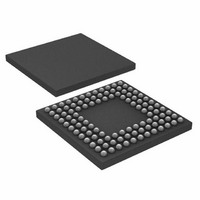
108-LFBGA, CSPBGA
Lead Free Status / RoHS Status
Lead free / RoHS Compliant
Eeprom Size
-
Lead Free Status / RoHS Status
Lead free / RoHS Compliant
Other names
ADUC7121BBCZ-RL
ADUC7121BBCZ-RLTR
ADUC7121BBCZ-RLTR
Available stocks
Company
Part Number
Manufacturer
Quantity
Price
Company:

Part Number:
ADUC7121BBCZ-RL
Manufacturer:
Analog Devices Inc
Quantity:
10 000


SPECIFICATIONS
AV
otherwise noted.
Table 1.
Parameter
ADC CHANNEL SPECIFICATIONS
ENDPOINT ERRORS
DYNAMIC PERFORMANCE
ANALOG INPUT
PADC0x INPUT
Resolution
Integral Nonlinearity
Differential Nonlinearity
DC Code Distribution
Offset Error
Offset Error Match
Gain Error
Gain Error Match
Signal-to-Noise Ratio (SNR)
Total Harmonic Distortion (THD)
Peak Harmonic or Spurious Noise
Channel-to-Channel Crosstalk
Input Voltage Ranges
Leakage Current
Input Capacitance
Full-Scale Input Range
Input Leakage at PADC0x
Resolution
Gain Error
Gain Drift
Offset
Offset Drift
PADC0x Compliant Range
ADC Power-Up Time
DC Accuracy
DD
All Channels Except IDACx
IDACx Channels Only
Differential Mode
Single-Ended Mode
= IOV
Channels
4
4
4
DD
4
= 3.0 V to 3.6 V, PV
1, 2
5
3, 4
4
DD
= 2.0 V ± 5%, V
Min
12
0.15
20
11
0.1
Typ
5
±0.6
±0.5
1
±2
1
±1
±2
±1
69
−78
−75
−80
±0.2
20
20
0.15
3
30
REF
= 2.5 V internal reference, f
Rev. 0 | Page 5 of 96
Max
±2
+1.4/−0.99
±5
±5
V
0 to V
AV
±1
1000
2
1
50
6
60
AV
CM
DD
DD
6
± V
− 1.5
− 1.2
REF
REF
/2
Unit
μs
Bits
LSB
LSB
LSB
LSB
% of full
scale
LSB
LSB
LSB
dB
dB
dB
dB
V
V
V
μA
pF
pF
μA
nA
Bits
%
ppm/°C
nA
pA/°C
V
CORE
= 41.78 MHz, T
Test Conditions/Comments
Eight acquisition clocks and f
2.5 V internal reference, not production tested
for PADC0 and PADC1 channels
2.5 V internal reference, guaranteed
monotonic
ADC input is a dc voltage
Internally unbuffered channels
f
internally unbuffered channels
Includes distortion and noise components
Measured on adjacent channels
See Table 38
Buffer bypassed
Buffer enabled
During ADC acquisition buffer bypassed
During ADC acquisition buffer enabled
28.3 kΩ resistor, PGA gain = 3, acquisition
time = 3.2 μs, pseudo differential mode
0.1% accuracy, 5 ppm external resistor for
current to voltage
PGA offset not included
IN
= 10 kHz sine wave, f
A
= −10°C to +95°C, unless
SAMPLE
= 1 MSPS,
ADC
ADuC7121
/2
Related parts for ADUC7121BBCZ-RL
Image
Part Number
Description
Manufacturer
Datasheet
Request
R

Part Number:
Description:
±1.7g Dual-Axis IMEMS Accelerometer Evaluation Board
Manufacturer:
Analog Devices Inc
Datasheet:

Part Number:
Description:
Inertial Sensor Evaluation System
Manufacturer:
Analog Devices Inc
Datasheet:
Part Number:
Description:
Manufacturer:
Analog Devices Inc
Datasheet:
Part Number:
Description:
Manufacturer:
Analog Devices Inc
Datasheet:
Part Number:
Description:
Manufacturer:
Analog Devices Inc
Datasheet:
Part Number:
Description:
Manufacturer:
Analog Devices Inc
Datasheet:
Part Number:
Description:
Manufacturer:
Analog Devices Inc
Datasheet:
Part Number:
Description:
Manufacturer:
Analog Devices Inc
Datasheet:
Part Number:
Description:
Manufacturer:
Analog Devices Inc
Datasheet:
Part Number:
Description:
Manufacturer:
Analog Devices Inc
Datasheet:
Part Number:
Description:
Manufacturer:
Analog Devices Inc
Datasheet:
Part Number:
Description:
Manufacturer:
Analog Devices Inc
Datasheet:
Part Number:
Description:
Manufacturer:
Analog Devices Inc
Datasheet: