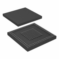
ADSP-BF527KBCZ-6 Analog Devices Inc, ADSP-BF527KBCZ-6 Datasheet - Page 48

ADSP-BF527KBCZ-6
Manufacturer Part Number
ADSP-BF527KBCZ-6
Description
ADSP-BF527 Processor,600Mhz,Ethernet,USB
Manufacturer
Analog Devices Inc
Series
Blackfin®r
Type
Fixed Pointr
Specifications of ADSP-BF527KBCZ-6
Interface
DMA, Ethernet, I²C, PPI, SPI, SPORT, UART, USB
Clock Rate
600MHz
Non-volatile Memory
ROM (32 kB)
On-chip Ram
132kB
Voltage - I/o
1.8V, 2.5V, 3.3V
Voltage - Core
1.10V
Operating Temperature
0°C ~ 70°C
Mounting Type
Surface Mount
Package / Case
289-CSPBGA
Lead Free Status / RoHS Status
Lead free / RoHS Compliant
For Use With
ADZS-BF527-MPSKIT - BOARD EVAL MEDIA PLAYER BF527ADZS-BF527-EZLITE - BOARD EVAL ADSP-BF527
Lead Free Status / RoHS Status
Lead free / RoHS Compliant
Available stocks
Company
Part Number
Manufacturer
Quantity
Price
Company:
Part Number:
ADSP-BF527KBCZ-6
Manufacturer:
Analog Devices Inc
Quantity:
10 000
Company:
Part Number:
ADSP-BF527KBCZ-6A
Manufacturer:
ALTERA
Quantity:
1 000
Company:
Part Number:
ADSP-BF527KBCZ-6A
Manufacturer:
ADI
Quantity:
210
Company:
Part Number:
ADSP-BF527KBCZ-6A
Manufacturer:
Analog Devices Inc
Quantity:
10 000
Part Number:
ADSP-BF527KBCZ-6A
Manufacturer:
ADI/亚德诺
Quantity:
20 000
Company:
Part Number:
ADSP-BF527KBCZ-6C2
Manufacturer:
Analog Devices Inc
Quantity:
10 000
External DMA Request Timing
Table 39
operations.
Table 38. External DMA Request Timing for ADSP-BF522/ADSP-BF524/ADSP-BF526 Processors
1
Table 39. External DMA Request Timing for ADSP-BF523/ADSP-BF525/ADSP-BF527 Processors
1
Parameter
Timing Requirements
t
t
t
t
Parameter
Timing Requirements
t
t
t
t
Because the external DMA control pins are part of the V
Because the external DMA control pins are part of the V
ADSP-BF522/ADSP-BF523/ADSP-BF524/ADSP-BF525/ADSP-BF526/ADSP-BF527
DS
DH
DMARACT
DMARINACT
DS
DH
DMARACT
DMARINACT
V
V
DDMEM
DDMEM
are NOT equal may require level shifting logic for correct operation.
are NOT equal may require level shifting logic for correct operation.
and
Figure 19
(ACTIVE HIGH)
(ACTIVE LOW)
DMARx Asserted to CLKOUT High Setup
CLKOUT High to DMARx Deasserted Hold Time
DMARx Active Pulse Width
DMARx Inactive Pulse Width
DMARx Asserted to CLKOUT High Setup
CLKOUT High to DMARx Deasserted Hold Time
DMARx Active Pulse Width
DMARx Inactive Pulse Width
DMAR0/1
CLKOUT
describe the External DMA Request
t
DS
DDEXT
DDEXT
t
DMARACT
power domain and the CLKOUT signal is part of the V
power domain and the CLKOUT signal is part of the V
Figure 19. External DMA Request Timing
Rev. B | Page 48 of 88 | May 2010
t
DH
Min
9.0
0.0
1.0 × t
1.75 × t
Min
8.0
0.0
1.0 × t
1.75 × t
t
DMARINACT
SCLK
SCLK
1.8 V Nominal
1.8 V Nominal
V
V
SCLK
SCLK
DDEXT
DDEXT
/V
/V
Max
Max
DDMEM
DDMEM
DDMEM
DDMEM
power domain, systems in which V
power domain, systems in which V
Min
6.0
0.0
1.0 × t
1.75 × t
Min
6.0
0.0
1.0 × t
1.75 × t
1
1
2.5/3.3 V Nominal
2.5/3.3 V Nominal
SCLK
SCLK
V
V
SCLK
SCLK
DDEXT
DDEXT
/V
/V
Max
Max
DDMEM
DDMEM
DDEXT
DDEXT
Unit
ns
Unit
ns
ns
ns
ns
ns
ns
ns
and
and


