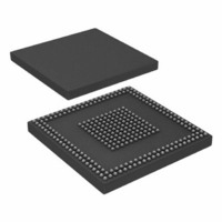
ADSP-BF527KBCZ-6 Analog Devices Inc, ADSP-BF527KBCZ-6 Datasheet - Page 22

ADSP-BF527KBCZ-6
Manufacturer Part Number
ADSP-BF527KBCZ-6
Description
ADSP-BF527 Processor,600Mhz,Ethernet,USB
Manufacturer
Analog Devices Inc
Series
Blackfin®r
Type
Fixed Pointr
Specifications of ADSP-BF527KBCZ-6
Interface
DMA, Ethernet, I²C, PPI, SPI, SPORT, UART, USB
Clock Rate
600MHz
Non-volatile Memory
ROM (32 kB)
On-chip Ram
132kB
Voltage - I/o
1.8V, 2.5V, 3.3V
Voltage - Core
1.10V
Operating Temperature
0°C ~ 70°C
Mounting Type
Surface Mount
Package / Case
289-CSPBGA
Lead Free Status / RoHS Status
Lead free / RoHS Compliant
For Use With
ADZS-BF527-MPSKIT - BOARD EVAL MEDIA PLAYER BF527ADZS-BF527-EZLITE - BOARD EVAL ADSP-BF527
Lead Free Status / RoHS Status
Lead free / RoHS Compliant
Available stocks
Company
Part Number
Manufacturer
Quantity
Price
Company:
Part Number:
ADSP-BF527KBCZ-6
Manufacturer:
Analog Devices Inc
Quantity:
10 000
Company:
Part Number:
ADSP-BF527KBCZ-6A
Manufacturer:
ALTERA
Quantity:
1 000
Company:
Part Number:
ADSP-BF527KBCZ-6A
Manufacturer:
ADI
Quantity:
210
Company:
Part Number:
ADSP-BF527KBCZ-6A
Manufacturer:
Analog Devices Inc
Quantity:
10 000
Part Number:
ADSP-BF527KBCZ-6A
Manufacturer:
ADI/亚德诺
Quantity:
20 000
Company:
Part Number:
ADSP-BF527KBCZ-6C2
Manufacturer:
Analog Devices Inc
Quantity:
10 000
SIGNAL DESCRIPTIONS
Signal definitions for the ADSP-BF52x processors are listed in
Table
package size and ball count, some balls have dual, multiplexed
functions. In cases where ball function is reconfigurable, the
default state is shown in plain text, while the alternate function
is shown in italics.
All pins are three-stated during and immediately after reset,
with the exception of the external memory interface, asynchro-
nous and synchronous memory control, and the buffered XTAL
output pin (CLKBUF). On the external memory interface, the
control and address lines are driven high, with the exception of
CLKOUT, which toggles at the system clock rate. During hiber-
nate, all outputs are three-stated unless otherwise noted in
Table
Table 10. Signal Descriptions
Signal Name
EBIU
ADDR19–1
DATA15–0
ABE1–0/SDQM1–0
AMS3–0
ARDY
AOE
ARE
AWE
SRAS
SCAS
SWE
SCKE
CLKOUT
SA10
SMS
ADSP-BF522/ADSP-BF523/ADSP-BF524/ADSP-BF525/ADSP-BF526/ADSP-BF527
10. In order to maintain maximum function and reduce
10.
Type Function
O
I/O
O
O
I
O
O
O
O
O
O
O
O
O
O
Rev. B | Page 22 of 88 | May 2010
Address Bus
Hardware Ready Control
SDRAM Clock Enable (Requires a pull-down if hibernate with SDRAM self-
SDRAM Clock Output
SDRAM A10 Signal
Data Bus
Byte Enables/Data Mask
Asynchronous Memory Bank Selects (Require pull-ups if hibernate is used.) A
Asynchronous Output Enable
Asynchronous Read Enable
Asynchronous Write Enable
SDRAM Row Address Strobe
SDRAM Column Address Strobe
SDRAM Write Enable
refresh is used.)
SDRAM Bank Select
All I/O pins have their input buffers disabled with the exception
of the pins that need pull-ups or pull-downs, as noted in
Table
It is strongly advised to use the available IBIS models to ensure
that a given board design meets overshoot/undershoot and sig-
nal integrity requirements. If no IBIS simulation is performed, it
is strongly recommended to add series resistor terminations for
all Driver Types A, C and D.
The termination resistors should be placed near the processor to
reduce transients and improve signal integrity. The resistance
value, typically 33 Ω or 47 Ω, should be chosen to match the
average board trace impedance.
Additionally, adding a parallel termination to CLKOUT may
prove useful in further enhancing signal integrity. Be sure to
verify overshoot/undershoot and signal integrity specifications
on actual hardware.
10.
Driver
Type
A
A
A
A
A
A
A
A
A
A
B
A
A
1


