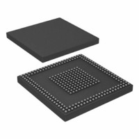
ADSP-BF527KBCZ-6 Analog Devices Inc, ADSP-BF527KBCZ-6 Datasheet - Page 42

ADSP-BF527KBCZ-6
Manufacturer Part Number
ADSP-BF527KBCZ-6
Description
ADSP-BF527 Processor,600Mhz,Ethernet,USB
Manufacturer
Analog Devices Inc
Series
Blackfin®r
Type
Fixed Pointr
Specifications of ADSP-BF527KBCZ-6
Interface
DMA, Ethernet, I²C, PPI, SPI, SPORT, UART, USB
Clock Rate
600MHz
Non-volatile Memory
ROM (32 kB)
On-chip Ram
132kB
Voltage - I/o
1.8V, 2.5V, 3.3V
Voltage - Core
1.10V
Operating Temperature
0°C ~ 70°C
Mounting Type
Surface Mount
Package / Case
289-CSPBGA
Lead Free Status / RoHS Status
Lead free / RoHS Compliant
For Use With
ADZS-BF527-MPSKIT - BOARD EVAL MEDIA PLAYER BF527ADZS-BF527-EZLITE - BOARD EVAL ADSP-BF527
Lead Free Status / RoHS Status
Lead free / RoHS Compliant
Available stocks
Company
Part Number
Manufacturer
Quantity
Price
Company:
Part Number:
ADSP-BF527KBCZ-6
Manufacturer:
Analog Devices Inc
Quantity:
10 000
Company:
Part Number:
ADSP-BF527KBCZ-6A
Manufacturer:
ALTERA
Quantity:
1 000
Company:
Part Number:
ADSP-BF527KBCZ-6A
Manufacturer:
ADI
Quantity:
210
Company:
Part Number:
ADSP-BF527KBCZ-6A
Manufacturer:
Analog Devices Inc
Quantity:
10 000
Part Number:
ADSP-BF527KBCZ-6A
Manufacturer:
ADI/亚德诺
Quantity:
20 000
Company:
Part Number:
ADSP-BF527KBCZ-6C2
Manufacturer:
Analog Devices Inc
Quantity:
10 000
NAND Flash Controller Interface Timing
Table 35
Page 45
Table 35. NAND Flash Controller Interface Timing
1
Parameter
Write Cycle
Switching Characteristics
t
t
t
t
t
t
t
t
t
t
t
Read Cycle
Switching Characteristics
t
t
t
t
t
Timing Requirements (ADSP-BF522/ADSP-BF524/ADSP-BF526)
t
t
Timing Requirements (ADSP-BF523/ADSP-BF525/ADSP-BF527)
t
t
Write Followed by Read
Switching Characteristics
t
WR_DLY and RD_DLY are defined in the NFC_CTL register.
CWL
CH
CLEWL
CLH
ALEWL
ALH
WP
WHWL
WC
DWS
DWH
CRL
CRH
RP
RHRL
RC
DRS
DRH
DRS
DRH
WHRL
ADSP-BF522/ADSP-BF523/ADSP-BF524/ADSP-BF525/ADSP-BF526/ADSP-BF527
1
1
1
1
1
describe NAND Flash Controller Interface operations.
and
Figure 13 on Page 43
ND_CE Setup Time to AWE Low
ND_CE Hold Time From AWE High
ND_CLE Setup Time to AWE Low
ND_CLE Hold Time From AWE high
ND_ALE Setup Time to AWE Low
ND_ALE Hold Time From AWE High
AWE Low to AWE high
AWE High to AWE Low
AWE Low to AWE Low
Data Setup Time for a Write Access
Data Hold Time for a Write Access
ND_CE Setup Time to ARE Low
ND_CE Hold Time From ARE High
ARE Low to ARE High
ARE High to ARE Low
ARE Low to ARE Low
Data Setup Time for a Read Transaction
Data Hold Time for a Read Transaction
Data Setup Time for a Read Transaction
Data Hold Time for a Read Transaction
AWE High to ARE Low
through
Figure 17 on
Rev. B | Page 42 of 88 | May 2010
Min
1.0 × t
3.0 × t
0.0
2.5 × t
0.0
2.5 × t
(WR_DLY +1.0) × t
4.0 × t
(WR_DLY +5.0) × t
(WR_DLY +1.5) × t
2.5 × t
1.0 × t
3.0 × t
(RD_DLY +1.0) × t
4.0 × t
(RD_DLY +5.0) × t
14.0
0.0
11.0
0.0
5.0 × t
SCLK
SCLK
SCLK
SCLK
SCLK
SCLK
SCLK
SCLK
SCLK
SCLK
1.8 V Nominal
– 4
– 4
– 4
– 4
– 4
– 4
– 4
– 4
– 4
– 4
V
DDEXT
SCLK
SCLK
SCLK
SCLK
SCLK
– 4
– 4
– 4
– 4
– 4
Min
1.0 × t
3.0 × t
0.0
2.5 × t
0.0
2.5 × t
(WR_DLY +1.0) × t
4.0 × t
(WR_DLY +5.0) × t
(WR_DLY +1.5) × t
2.5 × t
1.0 × t
3.0 × t
(RD_DLY +1.0) × t
4.0 × t
(RD_DLY +5.0) × t
10.0
0.0
8.0
0.0
5.0 × t
2.5/3.3 V Nominal
SCLK
SCLK
SCLK
SCLK
SCLK
SCLK
SCLK
SCLK
SCLK
SCLK
– 4
– 4
– 4
– 4
– 4
– 4
– 4
– 4
– 4
– 4
V
DDEXT
SCLK
SCLK
SCLK
SCLK
SCLK
– 4
– 4
– 4
– 4
– 4
Unit
ns
ns
ns
ns
ns
ns
ns
ns
ns
ns
ns
ns
ns
ns
ns
ns
ns
ns
ns
ns
ns


