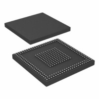
ADSP-BF527KBCZ-6 Analog Devices Inc, ADSP-BF527KBCZ-6 Datasheet - Page 36

ADSP-BF527KBCZ-6
Manufacturer Part Number
ADSP-BF527KBCZ-6
Description
ADSP-BF527 Processor,600Mhz,Ethernet,USB
Manufacturer
Analog Devices Inc
Series
Blackfin®r
Type
Fixed Pointr
Specifications of ADSP-BF527KBCZ-6
Interface
DMA, Ethernet, I²C, PPI, SPI, SPORT, UART, USB
Clock Rate
600MHz
Non-volatile Memory
ROM (32 kB)
On-chip Ram
132kB
Voltage - I/o
1.8V, 2.5V, 3.3V
Voltage - Core
1.10V
Operating Temperature
0°C ~ 70°C
Mounting Type
Surface Mount
Package / Case
289-CSPBGA
Lead Free Status / RoHS Status
Lead free / RoHS Compliant
For Use With
ADZS-BF527-MPSKIT - BOARD EVAL MEDIA PLAYER BF527ADZS-BF527-EZLITE - BOARD EVAL ADSP-BF527
Lead Free Status / RoHS Status
Lead free / RoHS Compliant
Available stocks
Company
Part Number
Manufacturer
Quantity
Price
Company:
Part Number:
ADSP-BF527KBCZ-6
Manufacturer:
Analog Devices Inc
Quantity:
10 000
Company:
Part Number:
ADSP-BF527KBCZ-6A
Manufacturer:
ALTERA
Quantity:
1 000
Company:
Part Number:
ADSP-BF527KBCZ-6A
Manufacturer:
ADI
Quantity:
210
Company:
Part Number:
ADSP-BF527KBCZ-6A
Manufacturer:
Analog Devices Inc
Quantity:
10 000
Part Number:
ADSP-BF527KBCZ-6A
Manufacturer:
ADI/亚德诺
Quantity:
20 000
Company:
Part Number:
ADSP-BF527KBCZ-6C2
Manufacturer:
Analog Devices Inc
Quantity:
10 000
ABSOLUTE MAXIMUM RATINGS
Stresses greater than those listed in
nent damage to the device. These are stress ratings only.
Functional operation of the device at these or any other condi-
Table 26. Absolute Maximum Ratings
1
2
3
4
5
Table 27. Maximum Duty Cycle for Input Transient Voltage
1
2
3
When programming OTP memory on the ADSP-BF522/
ADSP-BF524/ADSP-BF526 processors, the VPPOTP ball must
be set to the write value specified in the
for ADSP-BF522/ADSP-BF524/ADSP-BF526 Processors on
Page
write voltage may be applied (dependent on voltage and junc-
tion temperature) to VPPOTP over the lifetime of the part.
Therefore, maximum OTP memory programming time for the
Parameter
Internal Supply Voltage (V
Internal Supply Voltage (V
External (I/O) Supply Voltage (V
Input Voltage
Input Voltage
Input Voltage
Output Voltage Swing
I
Storage Temperature Range
Junction Temperature While Biased
V
–0.50
–0.70
–0.80
–0.90
–1.00
Applies to 100% transient duty cycle. For other duty cycles see
Applies only when V
Applies to balls SCL and SDA.
Applies to balls USB_DP, USB_DM, and USB_VBUS.
For more information, see description preceding
Applies to all signal balls with the exception of CLKIN, XTAL, VR
The individual values cannot be combined for analysis of a single instance of
Duty cycle refers to the percentage of time the signal exceeds the value for the
OH
ADSP-BF522/ADSP-BF523/ADSP-BF524/ADSP-BF525/ADSP-BF526/ADSP-BF527
EXT_WAKE1.
overshoot or undershoot. The worst case observed value must fall within one of
the voltages specified, and the total duration of the overshoot or undershoot
(exceeding the 100% case) must be less than or equal to the corresponding duty
cycle.
100% case. The is equivalent to the measured duration of a single instance of
overshoot or undershoot as a percentage of the period of occurrence.
IN
/I
Min (V)
OL
27. There is a finite amount of cumulative time that the
Current per Pin Group
2
1, 2
1, 2, 3
1, 2, 4
V
+3.80
+4.00
+4.10
+4.20
+4.30
DDEXT
IN
Max (V)
is within specifications. When V
DDINT
DDINT
5
2
) for ADSP-BF523/ADSP-BF525/ADSP-BF527 processors
) for ADSP-BF522/ADSP-BF524/ADSP-BF526 processors
DDEXT
Maximum Duty Cycle
100%
40%
25%
15%
10%
Table 26
/V
DDMEM
Operating Conditions
Table
)
may cause perma-
29.
DDEXT
Table
Rev. B | Page 36 of 88 | May 2010
is outside specifications, the range is V
OUT
27.
/
3
1
tions greater than those indicated in the operational sections of
this specification is not implied. Exposure to absolute maximum
rating conditions for extended periods may affect device
reliability.
ADSP-BF522/ADSP-BF524/ADSP-BF526 processors is shown
in
cessors do not have a similar restriction.
Table 28. Maximum OTP Memory Programming Time for
ADSP-BF522/ADSP-BF524/ADSP-BF526 Processors
Table 29
rent for a group of pins. Permanent damage can occur if this
value is exceeded. To understand this specification, if pins PH4,
PH3, PH2, PH1, and PH0 from group 1 in the
Groups
total current for those pins would be 10 mA. This would allow
up to 70 mA total that could be sourced or sunk by the remain-
ing pins in the group without damaging the device. For a list of
all groups and their pins, see the
table. Note that the V
per-pin maximum current requirements, see the
Characteristics for ADSP-BF522/ADSP-BF524/ADSP-BF526
Processors
ADSP-BF525/ADSP-BF527 Processors
V
6.9
7.0
7.1
PPOTP
Table
Voltage (V)
table, each were sourcing or sinking 2 mA each, the
28. The ADSP-BF523/ADSP-BF525/ADSP-BF527 pro-
specifies the maximum total source/sink (I
DDEXT
and
±0.2 V.
Electrical Characteristics for ADSP-BF523/
OL
25°C
6000 sec
2400 sec
1000 sec
and V
Rating
–0.3 V to +1.26 V
–0.3 V to +1.47 V
–0.3 V to +3.8 V
–0.5 V to +3.8 V
–0.5 V to +5.5 V
–0.5 V to +5.25 V
–0.5 V to V
80 mA (max)
–65°C to +150°C
+110°C
OL
Total Current Pin Groups
specifications have separate
Temperature (T
DDEXT
85°C
100 sec
44 sec
18 sec
tables.
/V
DDMEM
Total Current Pin
+0.5 V
Electrical
J
)
105°C
25 sec
12 sec
4.5 sec
OH
/I
OL
) cur-


