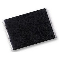
NANDO1GW3B2CN6 NUMONYX, NANDO1GW3B2CN6 Datasheet - Page 52

NANDO1GW3B2CN6
Manufacturer Part Number
NANDO1GW3B2CN6
Description
IC, FLASH, 1GB, 25µS, TSOP-48
Manufacturer
NUMONYX
Datasheet
1.NANDO1GW3B2CN6.pdf
(60 pages)
Specifications of NANDO1GW3B2CN6
Memory Type
FLASH
Memory Size
1GB
Access Time
25µS
Supply Voltage Range
2.7V TO 3.6V
Memory Case Style
TSOP
No. Of Pins
48
Operating Temperature Range
-40°C TO +85°C
Voltage, Vcc
3.3V
Memory Configuration
128M X 8
Rohs Compliant
Yes
DC and AC parameters
Figure 29. Program/erase enable waveforms
Figure 30. Program/erase disable waveforms
11.1
52/60
RB
RB
WP
WP
I/O
I/O
W
W
Ready/Busy signal electrical characteristics
Figure
signal. The value required for the resistor R
So,
where I
max is determined by the maximum value of t
High
32,
L
is the sum of the input currents of all the devices tied to the Ready/Busy signal. R
Figure 31
tVHWH
tVLWH
80h
80h
and
Figure 33
R P min
R P min 1.8V
R P min 3V
show the electrical characteristics for the Ready/Busy
=
(
-------------------------------------------------------------
(
V DDmax V OLmax
(
)
P
)
=
I OL
=
can be calculated using the following equation:
r
-------------------------- -
8mA
.
-------------------------- -
3mA
–
3.2V
+
1.85V
+
I L
+
I L
I L
10h
10h
NAND01G-B2B, NAND02G-B2C
)
ai12477
ai12478
P


