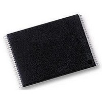
NANDO1GW3B2CN6 NUMONYX, NANDO1GW3B2CN6 Datasheet - Page 32

NANDO1GW3B2CN6
Manufacturer Part Number
NANDO1GW3B2CN6
Description
IC, FLASH, 1GB, 25µS, TSOP-48
Manufacturer
NUMONYX
Datasheet
1.NANDO1GW3B2CN6.pdf
(60 pages)
Specifications of NANDO1GW3B2CN6
Memory Type
FLASH
Memory Size
1GB
Access Time
25µS
Supply Voltage Range
2.7V TO 3.6V
Memory Case Style
TSOP
No. Of Pins
48
Operating Temperature Range
-40°C TO +85°C
Voltage, Vcc
3.3V
Memory Configuration
128M X 8
Rohs Compliant
Yes
Device operations
6.9
32/60
Read electronic signature
The device contains a manufacturer code and device code. To read these codes three steps
are required:
1.
2.
3.
Table 14.
Table 15.
NAND02GW3B2C
NAND01GW3B2B
NAND01GW4B2B
NAND01GR3B2B
NAND01GR4B2B
NAND02GR3B2C
NAND02GR4B2C
NAND02GW42C
Part number
One bus write cycle to issue the Read Electronic Signature command (90h)
One bus write cycle to input the address (00h)
Four bus read cycles to sequentially output the data (as shown in
signature).
I/O1-I/O0
I/O3-I/O2
I/O5-I/O4
I/O6
I/O7
I/O
Electronic signature
Electronic signature byte 3
Number of simultaneously
between multiple devices
Interleaved programming
Manufacturer
byte/word 1
Internal chip number
programmed pages
Cache program
0020h
0020h
code
20h
20h
Definition
Cell type
Device code
byte/word 2
AAh
DAh
BAh
CAh
A1h
B1h
C1h
F1h
Value
0 0
0 1
1 0
1 1
0 1
1 0
1 1
0 0
0 1
1 0
1 1
0 0
0
1
0
1
(see
byte/word 3
NAND01G-B2B, NAND02G-B2C
Table
80h
15)
Table 14: Electronic
Not supported
Not supported
Description
16-level cell
2-level cell
4-level cell
8-level cell
supported
supported
(see
byte/word 4
1
2
4
8
1
2
4
8
Table
1Dh
5Dh
1Dh
5Dh
15h
55h
15h
55h
16)


