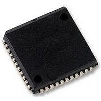
SC28L92A1A NXP Semiconductors, SC28L92A1A Datasheet - Page 9

SC28L92A1A
Manufacturer Part Number
SC28L92A1A
Description
UART, DUAL, 3.3V OR 5V, SMD, 28L92
Manufacturer
NXP Semiconductors
Datasheet
1.SC28L92A1B557.pdf
(73 pages)
Specifications of SC28L92A1A
No. Of Channels
2
Supply Voltage Range
2.97V To 3.63V, 4.5V To 5.5V
Operating Temperature Range
-40°C To +85°C
Digital Ic Case Style
PLCC
No. Of Pins
44
Svhc
No SVHC (18-Jun-2010)
Operating
RoHS Compliant
Data Rate
230.4Kilobaud
Uart Features
Programmable Channel Mode, Line Break Detection & Generation
Rohs Compliant
Yes
Available stocks
Company
Part Number
Manufacturer
Quantity
Price
Company:
Part Number:
SC28L92A1A
Manufacturer:
NXP
Quantity:
677
Company:
Part Number:
SC28L92A1A,512
Manufacturer:
NXP Semiconductors
Quantity:
10 000
Company:
Part Number:
SC28L92A1A,518
Manufacturer:
NXP Semiconductors
Quantity:
10 000
Company:
Part Number:
SC28L92A1A,529
Manufacturer:
NXP Semiconductors
Quantity:
10 000
Company:
Part Number:
SC28L92A1A529
Manufacturer:
NXP Semiconductors
Quantity:
135
NXP Semiconductors
Table 2.
SC28L92_7
Product data sheet
Symbol
I/M
D0
D1
D2
D3
D4
D5
D6
D7
CEN
WRN
RDN
A0
A1
A2
A3
RESET
INTRN
X1/CLK
X2
RxDA
RxDB
Pin
PLCC44 QFP44 HVQFN48
12
28
18
27
19
26
20
25
21
39
9
10
2
4
6
7
38
24
36
37
35
11
Pin description for 80xxx bus interface (Intel)
5.2 Pin description
11
22
12
21
13
20
14
19
15
33
3
4
40
42
44
1
32
18
30
31
29
5
7
23
14
22
15
21
16
20
17
35
3
4
44
46
48
1
34
19
32
33
31
5
Type
I
I/O
I/O
I/O
I/O
I/O
I/O
I/O
I/O
I
I
I
I
I
I
I
I
O
I
O
I
I
Rev. 07 — 19 December 2007
3.3 V/5.0 V Dual Universal Asynchronous Receiver/Transmitter
Description
Bus configuration: When HIGH or not connected configures the bus
interface to the conditions shown in this table.
Data bus: Bidirectional 3-state data bus used to transfer commands,
data and status between the DUART and the CPU. D0 is the least
significant bit.
Chip enable: Active LOW input signal. When LOW, data transfers
between the CPU and the DUART are enabled on D0 to D7 as
controlled by the WRN, RDN and A0 to A3 inputs. When HIGH, places
the D0 to D7 lines in the 3-state condition.
Write strobe: When LOW and CEN is also LOW, the contents of the
data bus is loaded into the addressed register. The transfer occurs on
the rising edge of the signal.
Read strobe: When LOW and CEN is also LOW, causes the contents
of the addressed register to be presented on the data bus. The read
cycle begins on the falling edge of RDN.
Address inputs: Select the DUART internal registers and ports for
read/write operations.
Reset: A HIGH level clears internal registers (SRA, SRB, IMR, ISR,
OPR and OPCR), puts OP0 to OP7 in the HIGH state, stops the
counter/timer, and puts channels A and B in the inactive state, with the
TxDA and TxDB outputs in the mark (HIGH) state. Sets MR pointer to
MR1. See
Interrupt request: Active LOW, open-drain, output which signals the
CPU that one or more of the eight maskable interrupting conditions are
true. This pin requires a pull-up device.
Crystal 1: Crystal or external clock input. A crystal or clock of the
specified limits must be supplied at all times. When a crystal is used, a
capacitor must be connected from this pin to ground (see
Crystal 2: Connection for other side of the crystal. When a crystal is
used, a capacitor must be connected from this pin to ground (see
Figure
be left open.
Channel A receiver serial data input: The least significant bit is
received first. See note on drive levels at block diagram
Channel B receiver serial data input: The least significant bit is
received first. See note on drive levels at block diagram
17). If X1/CLK is driven from an external source, this pin must
Figure
10.
SC28L92
© NXP B.V. 2007. All rights reserved.
(Figure
(Figure
Figure
1).
1).
17).
9 of 73


