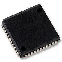
SC28L92A1A NXP Semiconductors, SC28L92A1A Datasheet - Page 28

SC28L92A1A
Manufacturer Part Number
SC28L92A1A
Description
UART, DUAL, 3.3V OR 5V, SMD, 28L92
Manufacturer
NXP Semiconductors
Datasheet
1.SC28L92A1B557.pdf
(73 pages)
Specifications of SC28L92A1A
No. Of Channels
2
Supply Voltage Range
2.97V To 3.63V, 4.5V To 5.5V
Operating Temperature Range
-40°C To +85°C
Digital Ic Case Style
PLCC
No. Of Pins
44
Svhc
No SVHC (18-Jun-2010)
Operating
RoHS Compliant
Data Rate
230.4Kilobaud
Uart Features
Programmable Channel Mode, Line Break Detection & Generation
Rohs Compliant
Yes
Available stocks
Company
Part Number
Manufacturer
Quantity
Price
Company:
Part Number:
SC28L92A1A
Manufacturer:
NXP
Quantity:
677
Company:
Part Number:
SC28L92A1A,512
Manufacturer:
NXP Semiconductors
Quantity:
10 000
Company:
Part Number:
SC28L92A1A,518
Manufacturer:
NXP Semiconductors
Quantity:
10 000
Company:
Part Number:
SC28L92A1A,529
Manufacturer:
NXP Semiconductors
Quantity:
10 000
Company:
Part Number:
SC28L92A1A529
Manufacturer:
NXP Semiconductors
Quantity:
135
NXP Semiconductors
Table 27.
MR1A is accessed when the channel A MR pointer points to MR1. The pointer is set to MR1 by RESET or by a set pointer
command applied via CR command 1. After reading or writing MR1A, the pointer will point to MR2A
[1]
SC28L92_7
Product data sheet
RxRTS
control
In block error mode, block error conditions must be cleared by using the error reset command (command 0x4) or a receiver reset.
7
MR1A - Mode Register 1 channel A (address 0x0) bit allocation
7.3.1.2 Mode Register 1 channel A (MR1A)
RxINT[1]
6
Table 28.
Bit
7
6
5
4 and 3
ERRORMODE
Symbol
RxRTS
RxINT[1]
ERRORMODE
PARITYMODE
MR1A - Mode Register 1 channel A (address 0x0) bit description
5
Rev. 07 — 19 December 2007
3.3 V/5.0 V Dual Universal Asynchronous Receiver/Transmitter
Description
Channel A receiver request to send control (flow control). This bit
controls the deactivation of the RTSAN output (OP0) by the receiver.
This output is normally asserted by setting OPR[0] and negated by
resetting OPR[0]. Proper automatic operation of flow control requires
OPR[0] (channel A) or OPR[1] (channel B) to be set to logic 1.
RxRTS = 1 causes RTSAN to be negated (OP0 is driven to a
logic 1 [V
full. This is the beginning of the reception of the 9th byte. If the FIFO is
not read before the start of the 10th or 17th byte, an overrun condition
will occur and the 10th or 17th or 17th byte will be lost. However, the
bit in OPR[0] is not reset and RTSAN will be asserted again when an
empty FIFO position is available. This feature can be used for flow
control to prevent overrun in the receiver by using the RTSAN output
signal to control the CTSN input of the transmitting device.
Bit 1 of the receiver interrupt control. See description of RxINT[2] in
Table 25
Channel A error mode select.
This bit selects the operating mode of the three FIFOed status bits
(FE, PE, received break) for channel A. In the character mode, status
is provided on a character-by-character basis; the status applies only
to the character at the top of the FIFO. In the block mode, the status
provided in the SR for these bits is the accumulation (logic OR) of the
status for all characters coming to the top of the FIFO since the last
reset error command for channel A was issued.
Channel A parity mode select
If with parity or force parity is selected a parity bit is added to the
transmitted character and the receiver performs a parity check on
incoming data MR1A[4:3] = 11 selects channel A to operate in the
special multi-drop mode described in
(9-bit or
4
PARITYMODE
0 = No RTS control
1 = RTS control
0 = character
1 = block
00 = with parity
01 = force parity
10 = no parity
11 = multi-drop special mode
wake-up)”.
and
CC
]) upon receipt of a valid start bit if the channel A FIFO is
Table
3
26.
PARITYTYPE
2
Section 6.3.10 “Multi-drop mode
[1]
bits per character
1
.
SC28L92
© NXP B.V. 2007. All rights reserved.
0
28 of 73


