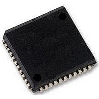
SC28L92A1A NXP Semiconductors, SC28L92A1A Datasheet - Page 71

SC28L92A1A
Manufacturer Part Number
SC28L92A1A
Description
UART, DUAL, 3.3V OR 5V, SMD, 28L92
Manufacturer
NXP Semiconductors
Datasheet
1.SC28L92A1B557.pdf
(73 pages)
Specifications of SC28L92A1A
No. Of Channels
2
Supply Voltage Range
2.97V To 3.63V, 4.5V To 5.5V
Operating Temperature Range
-40°C To +85°C
Digital Ic Case Style
PLCC
No. Of Pins
44
Svhc
No SVHC (18-Jun-2010)
Operating
RoHS Compliant
Data Rate
230.4Kilobaud
Uart Features
Programmable Channel Mode, Line Break Detection & Generation
Rohs Compliant
Yes
Available stocks
Company
Part Number
Manufacturer
Quantity
Price
Company:
Part Number:
SC28L92A1A
Manufacturer:
NXP
Quantity:
677
Company:
Part Number:
SC28L92A1A,512
Manufacturer:
NXP Semiconductors
Quantity:
10 000
Company:
Part Number:
SC28L92A1A,518
Manufacturer:
NXP Semiconductors
Quantity:
10 000
Company:
Part Number:
SC28L92A1A,529
Manufacturer:
NXP Semiconductors
Quantity:
10 000
Company:
Part Number:
SC28L92A1A529
Manufacturer:
NXP Semiconductors
Quantity:
135
NXP Semiconductors
16. Revision history
Table 72.
SC28L92_7
Product data sheet
Document ID
SC28L92_7
Modifications:
SC28L92_6
SC28L92_5
(9397 750 13125)
SC28L92_4
(9397 750 06796)
SC28L92_3
(9397 750 05979)
SC28L92_2
(9397 750 04465)
SC28L92_1
Revision history
Release date
20071219
20060426
20040907
20000121
19990507
19981005
-
•
•
•
•
•
•
•
•
•
•
•
The format of this data sheet has been redesigned to comply with the new identity
guidelines of NXP Semiconductors.
Legal texts have been adapted to the new company name where appropriate.
added HVQFN48 package option
Figure 1 “Block diagram (80xxx mode)”
– reversed position of “control” and “timing” notations
– reversed direction of signals IP0 to IP6
Figure 2 “Block diagram (68xxx mode)”
– corrected pin name from “RDN” to “R/WN”
– corrected pin name from “WRN” to “IACKN”
– corrected pin name from “RESET” to “RESETN”
– added signal DACKN
– reversed position of “control” and “timing” notations
– reversed direction of signals IP0 to IP5
Section 6.1.4 “FIFO
– 1
– 1
– 2
Table 24 “MR0A - Mode Register 0 channel A (address 0x0) bit
– description for bit 3: added “for channel A and channel B”
– description for bits [2:0]: in last line of description, changed “MR2[2:0]” to “MR0[2:0]”
Table
– added
– removed “(default)” (2 places)
Table
– added
– removed “(default)” (2 places)
Section 7.3.1.4 “Mode Register 0 channel B
Table 64 “Limiting
st
st
nd
25:
26:
paragraph, 4
paragraph, added new 6
paragraph: changed “MR0[3] bit” to “MR0A[3] bit”
Table note 1
Table note 1
Data sheet status
Product data sheet
Product data sheet
Product specification
Product specification
Product specification
Preliminary specification
-
Rev. 07 — 19 December 2007
3.3 V/5.0 V Dual Universal Asynchronous Receiver/Transmitter
values”: added specifications for HVQFN48 package
th
configuration”:
sentence: changed “MR0[3] bit” to “MR0A[3] bit”
th
sentence
modified:
modified:
Change notice
-
(MR0B)”, 2
-
-
-
-
-
-
nd
paragraph re-written.
description”:
Supersedes
SC28L92_6
SC28L92_5
(9397 750 13125)
SC28L92_4
(9397 750 06796)
SC28L92_3
(9397 750 05979)
SC28L92_2
(9397 750 04465)
SC28L92_1
-
SC28L92
© NXP B.V. 2007. All rights reserved.
71 of 73


