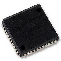
SC28L92A1A NXP Semiconductors, SC28L92A1A Datasheet - Page 10

SC28L92A1A
Manufacturer Part Number
SC28L92A1A
Description
UART, DUAL, 3.3V OR 5V, SMD, 28L92
Manufacturer
NXP Semiconductors
Datasheet
1.SC28L92A1B557.pdf
(73 pages)
Specifications of SC28L92A1A
No. Of Channels
2
Supply Voltage Range
2.97V To 3.63V, 4.5V To 5.5V
Operating Temperature Range
-40°C To +85°C
Digital Ic Case Style
PLCC
No. Of Pins
44
Svhc
No SVHC (18-Jun-2010)
Operating
RoHS Compliant
Data Rate
230.4Kilobaud
Uart Features
Programmable Channel Mode, Line Break Detection & Generation
Rohs Compliant
Yes
Available stocks
Company
Part Number
Manufacturer
Quantity
Price
Company:
Part Number:
SC28L92A1A
Manufacturer:
NXP
Quantity:
677
Company:
Part Number:
SC28L92A1A,512
Manufacturer:
NXP Semiconductors
Quantity:
10 000
Company:
Part Number:
SC28L92A1A,518
Manufacturer:
NXP Semiconductors
Quantity:
10 000
Company:
Part Number:
SC28L92A1A,529
Manufacturer:
NXP Semiconductors
Quantity:
10 000
Company:
Part Number:
SC28L92A1A529
Manufacturer:
NXP Semiconductors
Quantity:
135
NXP Semiconductors
Table 2.
SC28L92_7
Product data sheet
Symbol
TxDA
TxDB
OP0
OP1
OP2
OP3
OP4
OP5
OP6
OP7
IP0
IP1
IP2
IP3
IP4
IP5
IP6
V
CC
Pin
PLCC44 QFP44 HVQFN48
33
13
32
14
31
15
30
16
29
17
8
5
40
3
43
42
41
44
Pin description for 80xxx bus interface (Intel)
28
6
27
7
26
8
25
9
24
10
2
43
34
41
37
36
35
38, 39
30
8
29
9
28
10
27
11
26
12
2
47
38
45
41
40
39
42
Type
O
O
O
O
O
O
O
O
O
O
I
I
I
I
I
I
I
Pwr
Rev. 07 — 19 December 2007
3.3 V/5.0 V Dual Universal Asynchronous Receiver/Transmitter
Description
Channel A transmitter serial data output: The least significant bit is
transmitted first. This output is held in the Mark condition when the
transmitter is disabled, Idle or when operating in local loopback mode.
See note on drive levels at block diagram
Channel B transmitter serial data output: The least significant bit is
transmitted first. This output is held in the Mark condition when the
transmitter is disabled, Idle, or when operating in local loopback mode.
See note on drive levels at block diagram
Output 0: General purpose output or channel A request to send
(RTSAN, active LOW). Can be deactivated automatically on receive or
transmit.
Output 1: General-purpose output or channel B request to send
(RTSBN, active LOW). Can be deactivated automatically on receive or
transmit.
Output 2: General purpose output, or channel A transmitter 1 or 16
clock output, or channel A receiver 1 clock output.
Output 3: General purpose output or open-drain, active LOW
counter/timer output or channel B transmitter 1 clock output, or
channel B receiver 1 clock output.
Output 4: General purpose output or channel A open-drain, active
LOW, RxA interrupt ISR[1] output.
Output 5: General-purpose output or channel B open-drain, active
LOW, RxB interrupt ISR[5] output.
Output 6: General purpose output or channel A open-drain, active
LOW, TxA interrupt ISR[0] output.
Output 7: General-purpose output, or channel B open-drain, active
LOW, TxB interrupt ISR[4] output.
Input 0: General purpose input or channel A clear to send active LOW
input (CTSAN).
Input 1: General purpose input or channel B clear to send active LOW
input (CTSBN).
Input 2: General-purpose input or counter/timer external clock input.
Input 3: General purpose input or channel A transmitter external clock
input (TxCA). When the external clock is used by the transmitter, the
transmitted data is clocked on the falling edge of the clock.
Input 4: General purpose input or channel A receiver external clock
input (RxCA). When the external clock is used by the receiver, the
received data is sampled on the rising edge of the clock.
Input 5: General purpose input or channel B transmitter external clock
input (TxCB). When the external clock is used by the transmitter, the
transmitted data is clocked on the falling edge of the clock.
Input 6: General purpose input or channel B receiver external clock
input (RxCB). When the external clock is used by the receiver, the
received data is sampled on the rising edge of the clock.
Power Supply: 3.3 V
…continued
10 % or 5 V
10 % supply input.
(Figure
(Figure
1).
1).
SC28L92
© NXP B.V. 2007. All rights reserved.
10 of 73


